Reliability optimization for the next generation of LED-based smart and comfortable lighting solutions
The incandescent light bulb, patented by Thomas Edison in 1880, is now an endangered species. It is condemned to extinction because it no longer meets the technical requirements of the 21st century. A conventional light bulb converts just 5 % of the energy it consumes into light, while the remaining 95 % is emitted as heat. That is why Europe has banned all frosted and high-energy incandescent light bulbs from manufacturing and selling in the EU member states in 2008.
Today, light-emitting diodes, or LEDs for short, have an efficiency of up to 90 %. They are smaller, more flexible and offer far more scope for innovative lighting design solutions. On the other hand, the manufacturing costs of LED-based lighting systems have still been relatively high and the light produced often failed to meet customer requirements. An interdisciplinary team of experts drawn from 30 European companies and research institutes has therefore participated in the EU’s EnLight project, which aimed for creating sustainable and energy-efficient lighting systems based on LEDs that emit light compatible with all the situation-specific requirements for human comfort.
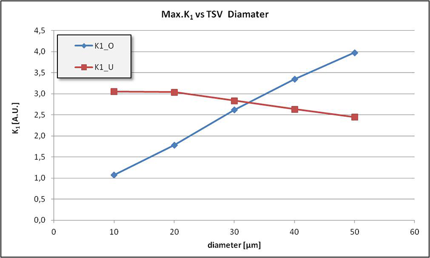
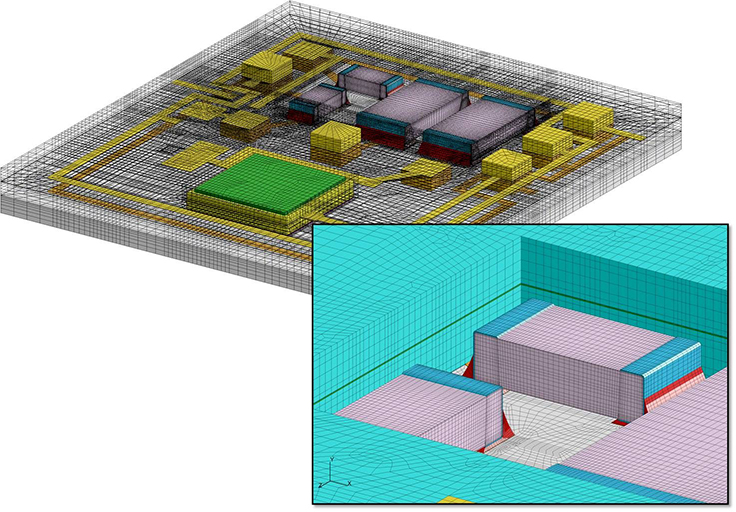
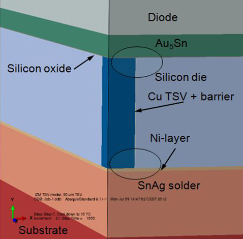
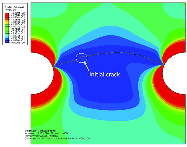
Within this project, members of the Micro Materials Center at Fraunhofer ENAS have developed and implemented a novel strategy of virtual prototyping that allows assessing the reliability prospects of new designs and manufacturing processes already prior to any first fabrication of the systems. This way, the physical development can directly start with the most promising option – avoiding time consuming learning cycles. Particular attention has been paid to 3D integration as important key technology for advanced LED lighting solutions. Within this scope, thermal through silicon vias (TSV) are seen as elegant way to efficiently transfer the heat from the power LED component to the heat spreading structures on the backside of a substrate. However, the thermal mismatch between the copper of the TSV and silicon of the dies also generates novel challenges for the system reliability as well as for the reliability analysis and prediction. Multiple failure modes occur simultaneously: interface delamination, bulk cracking and material fatigue. Therefore, the new simulation strategy has been developed for the complex virtual assessment. The strategy utilizes an interaction integral approach within the simulative DoE studies based on X-FEM fracture mechanics analysis in order to anticipate the crack propagation paths and speeds in silicon realistically for each design and process option. The DoE-based response surface methodology provided all means for a very efficient assessment and pre-optimization of the intended thermal TSV-approach for all the various LED packaging applications. The new assessment method of virtual prototyping delivers ‘first time right’ design solutions in minimum time. It speeds up the development cycle for new LED-based lighting solutions substantially.
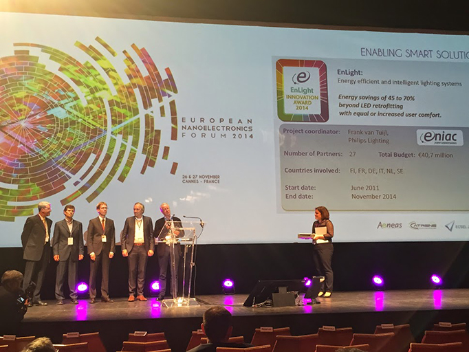
Even with its modest contribution to the over-all project results, the team involved at Fraunhofer ENAS is very proud that EnLight received the 2014 ENIAC Innovation Award at the European Nanoelectronics forum in Cannes on November 26-27.
The award was presented by Dr. Andreas Wild and Dr. Yves Gigase, respectively Executive Director and Head of Operations, formerly of the ENIAC JU and now of the ECSEL Joint Undertaking that has now taken up the support of the ENIAC projects.
In his speech, Dr. Wild highlighted once more the importance of semiconductor technology as a core European competence, which fully delivers on its promise of innovation when taken up by leading actors along the full value chain; from device suppliers, software and integration specialists to system developers. In this way, the EnLight project has been exemplary in bringing together such key actors in a project of significant size (more than 41 million euros R&D investment) to achieve results of genuinely high value to the partners.
 Fraunhofer Institute for Electronic Nano Systems