Parameter identification by nanoindenter
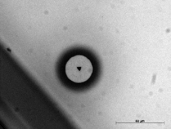
Continual downsizing and the integration of multiple features into microelectronic circuits continuously increase their structural complexity. This is also the case for through silicon vias (TSV), in which the mechanical characterization of copper in the TSV is not feasible with classical methods of material characterization due to the small size. However, the instrumented nanoindentation is a promising approach when using several indenter tips. Unique solutions for elastic-plastic material behavior were achieved using Berkovich and Cube Corner Indenter tips. The force displacement curves were modeled by the finite elements method and simulated under the assumption of isotropic hardening (Ramberg-Osgood). After comparing the results, it was possible to specify the hardening exponent and yield strength. The presented method enables a fast prediction of the material behavior in a first approach. With the help of finite element simulations it was possible to estimate the risk of delamination in the BEoL stack around copper TSVs where materials with large thermal expansion differences interact.
 Fraunhofer Institute for Electronic Nano Systems