Our scanning electron microscopes enable the precise analysis of various materials and samples. These include, among others:
Scanning Electron Microsopy - Manual Analysis


Layer thickness and defect characterization, particularly FIB: Analysis of micro defects by creating local precision cuts using a focused ion beam (FIB). The selective removal or ablation of material allows cross-sectioning of samples for SEM imaging. FIB cross-sectioning for visualization of deep structures, identification of delaminations and determination of layer thicknesses.


Surface characterization: High-resolution SEM images of surface structures and topography of various samples such as 4" to 8" wafers, fragments, semiconductor devices, embedded samples (SEM sections) and many more.

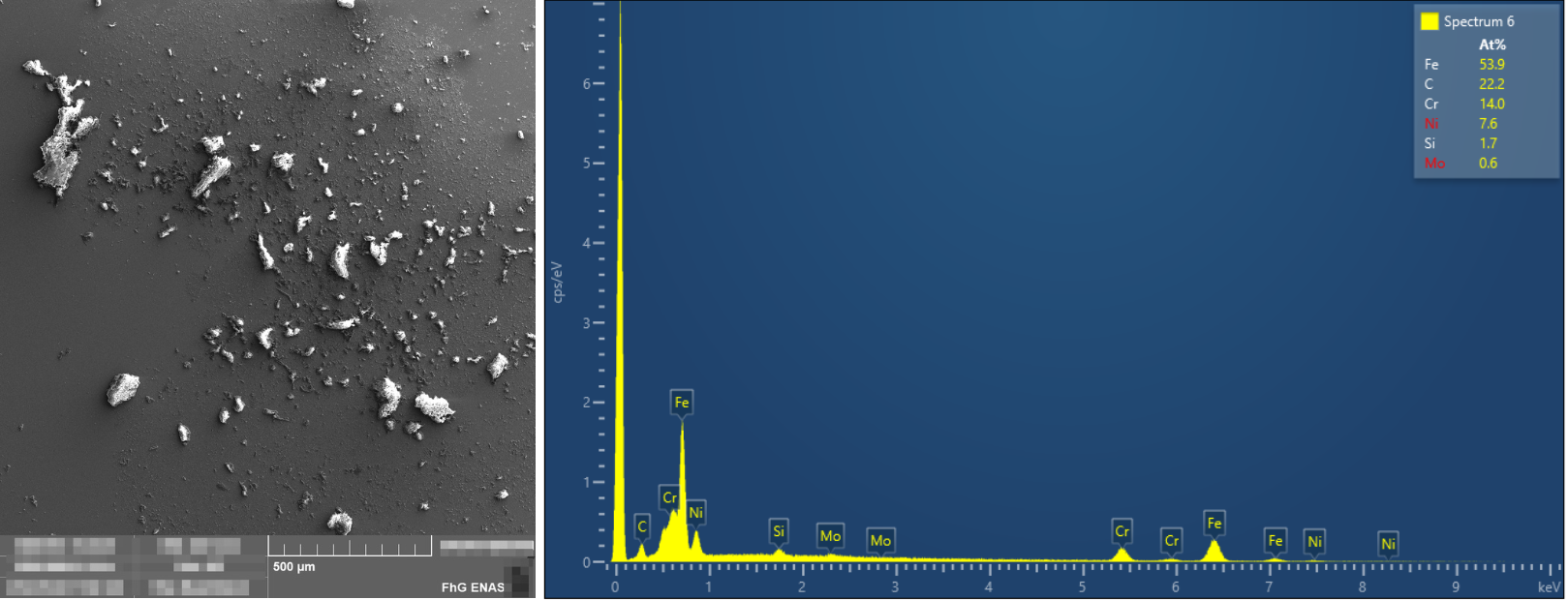
Element characterization: Energy dispersive x-ray spectroscopy (EDX, EDS) analysis of chemical material composition to determine the elemental distribution on the surface of a sample (EDX spectrum) as well as the creation of elemental distribution maps (mapping). It enables the chemical analysis of materials by measuring the characteristic x-ray radiation generated by the elements in the sample area of the SEM.
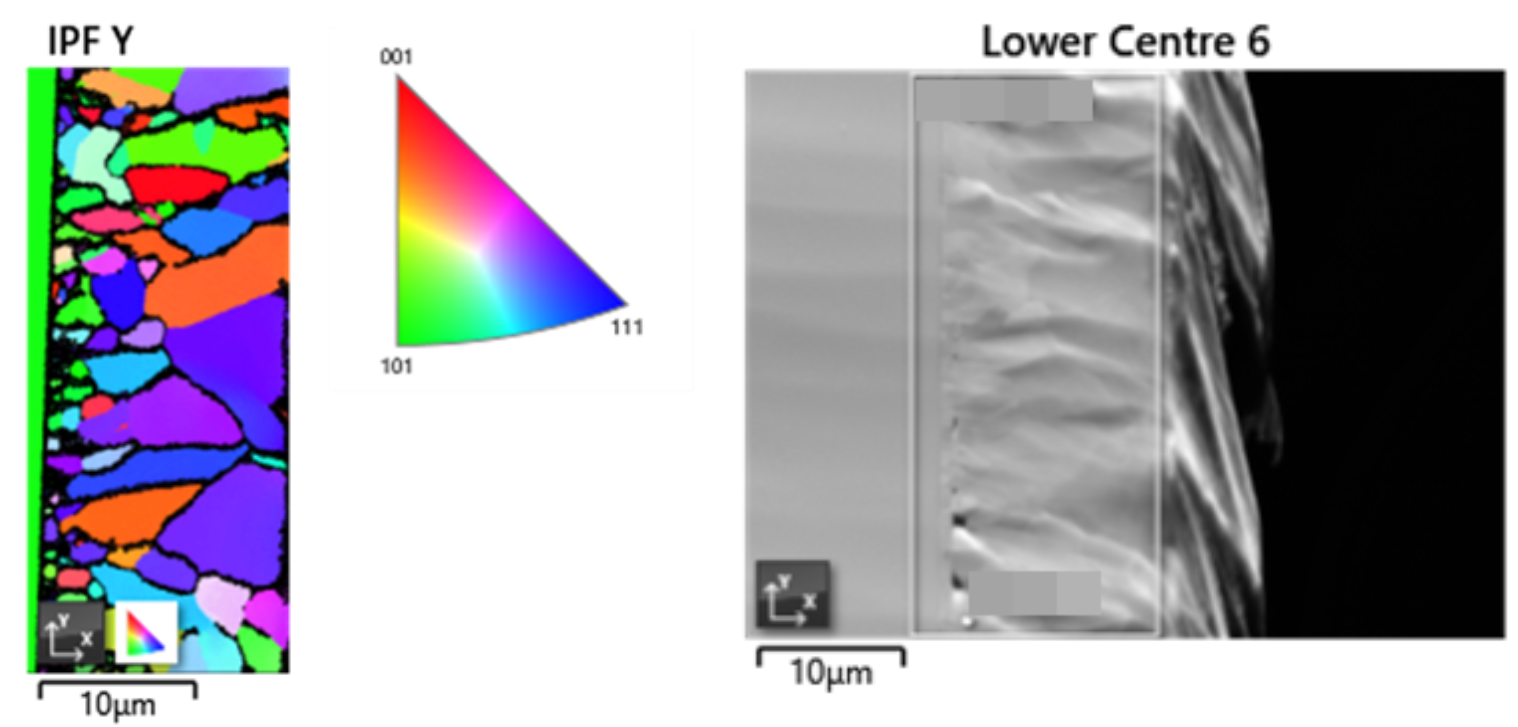
Crystallographic material characterization: Phase, texture and grain size analysis using electron backscatter diffraction (EBSD). This method provides information on grain orientation, lattice deformations as well as phase identification.
 Fraunhofer Institute for Electronic Nano Systems