 Fraunhofer Institute for Electronic Nano Systems
Fraunhofer ENAS and Tohoku University Sendai present joint research results at the nano tech 2014 in Tokyo
The researchers of the Fraunhofer Institute for Electronic Nano Systems ENAS and the Fraunhofer Project Center in Sendai show joint research results for SLID bonding at the nano tech in Tokyo from January 29 to 31, 2014. For the first time in Japan, the Fraunhofer researchers demonstrate a printed test card for analyzing the cholesterol content.
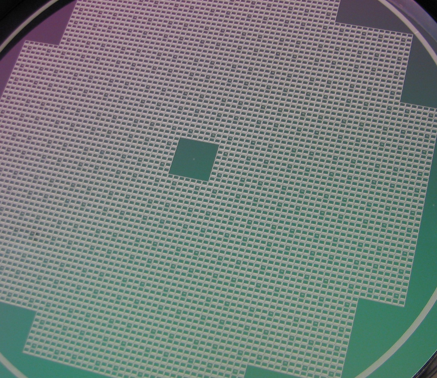
Chemnitz researchers of Fraunhofer ENAS and the Technische Universität Chemnitz attend the world‘s largest nanotechnology exhibiton in Tokyo. Together with the Fraunhofer Project Center „NEMS/MEMS Devices and Manufacturing Technologies at Tohoku University“ from Sendai, the scientists show researchresults on the so called Solid-Liquid Interdiffusion Bonding (SLID Bonding) at wafer level. This packaging technology is already established at chip and component level. Now it will be developed for wafer level packaging of MEMS (micro-electro-mechanical systems) and 3D integration. SLID bonding has some advandages. The process temperatures are between 100 °C and 300 °C depending on the material partners. The researchers focus on the deposition of nanolayers of these materials to reduce the melting point and to use nanoscale effects for packaging. Furthermore hermetical encapsulation of MEMS and electrical conductivity can be reached by using this packaging technology. SLID bonding is realized by a short liquid phase of one low melting metal and the immediate solidification caused by diffusion and intermixing with a second, high melting metal (Solid-Liquid Interdiffusion – SLID). The investigations are focused on the selection of suitable material combinations, the precise deposition of layers and layer systems as well as the right bonding parameters inclusively surface pretreatment.
The German researchers of Fraunhofer ENAS and Technische Universität Chemnitz cooperate with partners of the Tohoku University in Sendai, Japan, since several years. In 2012, the Fraunhofer Project Center „NEMS/MEMS Devices and Manufacturing Technologies at Tohoku University“ was established to realize joint research and development, training and technology transfer. Directors of the project center are Prof. Dr. Thomas Gessner, director of Fraunhofer ENAS and the Center for Microtechnologies at the TU Chemnitz, as well as Prof. Dr. Masayoshi Esashi and Prof. Dr. Shuji Tanaka from the Tohoku University in Sendai.
Prof. Gessner will present ressource efficient innovations based on nano technologies at the Seeds & Needs Seminar (B) on January 30th. For the first time, he will show results obtained within the cluster of excellence merge of the TU Chemnitz. The main object of the cluster is the fusion of fundamental technologies suitable for the resource-efficient massproduction of lightweight structures of high-performance and functional density. In order to make the structures much more intelligent, microsystems, smart sensors, actuators and electronics will be integrated. In his presentation Prof. Gessner is focusing on the integration of sensors and actuators in hybrid structures for structural health monitoring and the development and manufacturing of foil-based touch-sensitive sensors based on composites.
Experts on the printing sector will meet at the Printable Electronics 2014, which is also held as concurrent show in Tokyo. For the first time, Fraunhofer ENAS shows a diagnostic device for measuring cholesterol content in the blood. The system is a joint development of Fraunhofer ENAS with the University of the West of England, the University of Liverpool, the Dublin City University, Alere and VTT in the EU project SIMS. The system integrates printed components – biosensors, displays and batteries – onto a flexible plastic substrate. The diagnostic device is powered by a printed battery. Researchers at the department Printed Functionalities at the Fraunhofer ENAS developed this battery based on a layer system of zinc and manganese dioxide. The battery is produced by screen printing. The project partners aim the manufacturing of low-priced medical one way test by using low-cost printing technologies.
Last modified: