Temporary wafer bonding for MEMS devices


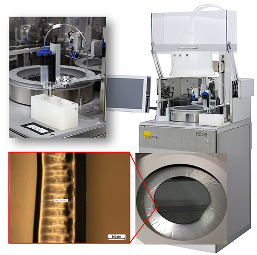
3D integrated sensors or electronic systems consist of individual components which are vertically stacked and have electrical connections. Therefore, new technologies and the development of new processes are essential. One key technology is the back thinning after temporary wafer bonding. The 3D integration requires the wafer thinning of both MEMS and CMOS devices. Ultrathin silicon wafers up to 100 µm have low stability, low bending stiffness, and are fragile. In order to enable the fabrication of thin Si substrates or to stabilize them during the mechanical processing, it is necessary to temporarily attach a device wafer to a carrier wafer. Different processes have been established recently. One method for temporary wafer bonding is provided by Brewer Science, which is called zone bonding. This method involves the spin coating of a device wafer with an adhesive. The carrier is coated with another adhesive at the wafer edge. The remaining area in the center of the carrier wafer is with an anti-sticking layer. The spin coating of the device and the carrier wafers is carried on the semiautomatic RCD8 spin coater from SUSS MicroTec. The device wafer is prepared by the deposition of a layer thickness of 15 – 30 µm of an adhesive (ZoneBOND® 5150-30). The first step of the carrier wafer fabrication on the RCD8 is the formation of a zone on the wafer edge with the adhesive ZoneBOND® EM 2320-15. An exact centering of the carrier wafer on the vacuum chuck is important for the wafer edge zone to get uniform coating. The thickness of the layer is in the range of 0.5 – 3 μm. After baking at 220 °C, an anti-stick layer (ZoneBOND® Z1 3500-02) is dispensed on the center of the carrier wafer. Figure 1 shows the coating system with a fabricated carrier wafer by using the ZoneBOND® method.
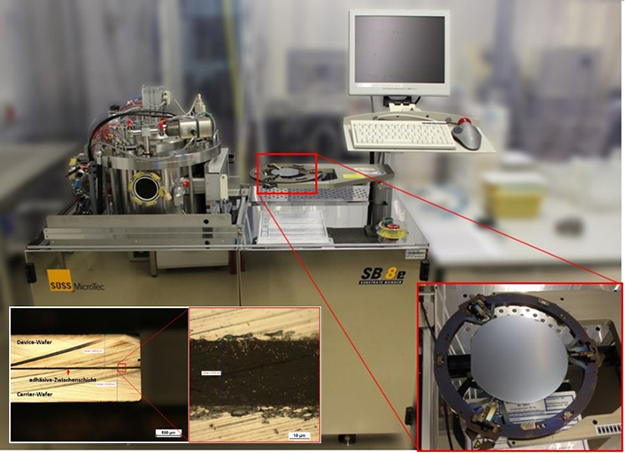
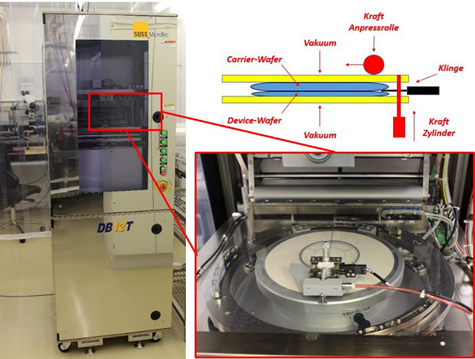
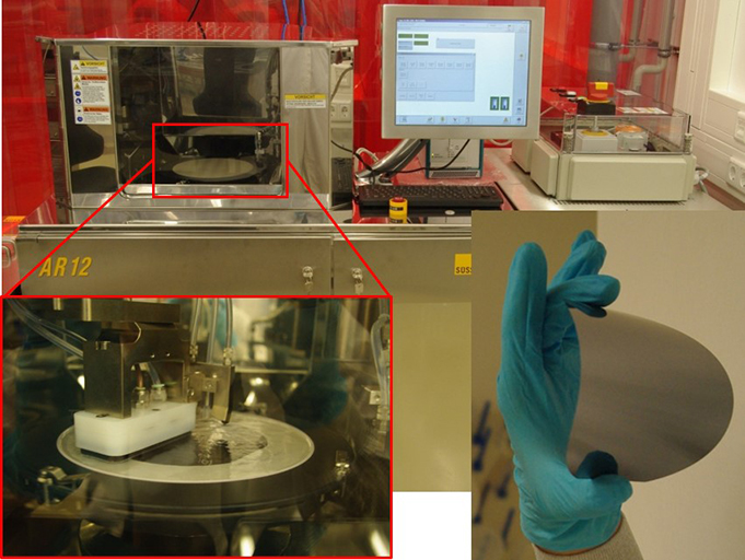
The subsequent adhesive wafer bonding is realized by using a SUSS MicroTec SB8 wafer bonder. The adhesive wafer bonding is carried out under vacuum (process pressure < 5 mbar) with a 170 kN/m2 bonding pressure. During the bonding process, two zones are formed. In the middle of the wafer is a fragile adhesive region (zone 1). In contrast to the zone 1, there is a strong adhesive area on the wafer edge (zone 2). Figure 2 shows a wafer stack on a 6 inch fixture before bonding in the SB8e and the formed intermediate layer after the adhesive wafer bonding. After chemical, mechanical and thermal processes (T < 250 °C), the edge zone of the strong adhesive area is released with limonene or mesitylene. Then, the wafer stack with the device wafer face down is mounted on a tape frame and placed in a debonding system (DB12T from SUSS MicroTec). In the DB12T debonder, the mounted wafer stack is fixed on both sides by vacuum. The mechanical separation of device and carrier wafers is done by a blade over the C-cut at the wafer edge. The carrier wafer is clamped over the blade and vertically moved on a flex plate over power cylinder at room temperature (see Fig. 3). In the final step, the device wafer on the mounted tape frame and the carrier wafer are cleaned. Similar to the edge release process, the cleaning is performed in the SUSS MicroTec AR12 module with limonene or mesitylene. With this process flow, a thinned wafer (150 mm diameter) down to 50 µm can be fabricated (see Fig. 4). In parallel, Brewer Science presented a new temporary wafer bonding method, called BrewerBOND® process. The process flow, particularly, the preparation of carrier wafer is significantly simplified for the BrewerBOND® method. Compared to ZoneBOND®, the anti-sticking layer is coated on the complete carrier wafer. As a result, wet chemical edge release before debonding is not required. The focus of different projects in cooperation with SUSS MicroTec is to clarify suitable process parameters for wafer coating using a new adhesive (e.g. BrewerBOND® 305) for the device wafer as well as a new anti-sticking layer (e.g. BrewerBOND® 510) for the carrier wafer. Preliminary investigations show that the bond strength is sufficient in terms of mechanical, thermal and chemical stress.
 Fraunhofer Institute for Electronic Nano Systems