Light-emitting diodes based on quantum dots for integration in plastic material


In recent years, colloidal quantum dots (QDs) have strongly attracted attention in the field of lighting and display technologies [1]. These are crystals from inorganic semiconductors in the size of a few nanometers which leads to quantum effects which dictate their optical and electronical behavior. The smaller these crystals get, the more confined are the charge carriers which increases the gap between the energy bands of the QDs. This means the wavelength of the emitted light of the QDs can be tuned by their size. Other advantages are the high quantum efficiency, small full width at half maximum (FWHM), chemical stability, and the possibility to process from a solution.
These advantages are used in light-emitting diodes based on QDs (QD-LEDs) which give them a few benefits over their organic counterparts. It is possible to produce QD-LEDs in nearly every wavelength of the visible light with the same material by using different sized QDs as the emitting layer and the FWHM is much smaller (30 – 40 nm for QD-LEDs and 60 – 120 nm for organic emitters). Furthermore, the progress of QD-LEDs has been enormous in the past 15 years and external quantum efficiency (EQE) values of over 20 % [2] were reached. Because of these special properties of the light, QD-LEDs are interesting for use in different fields as lightning, as for example spectroscopically sensors.
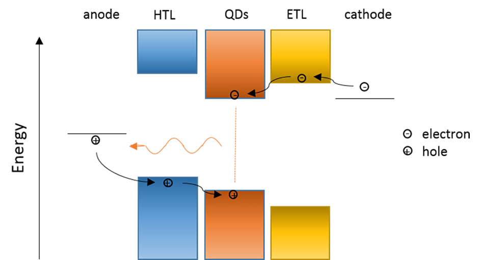
The typical setup of a QD-LED is a layer of QDs sandwiched between a hole transport layer (HTL) and an electron transport layer, as well as the electrodes (Fig.1). The highest efficiencies were reached using an organic HTL and an inorganic ETL. For deposition of these layers, the Fraunhofer ENAS provides different opportunities, both vapor deposition techniques (e.g. sputtering, thermal evaporation or molecular beam) and solution-based techniques (e.g. inkjet printing or spin coating). With these possibilities the QD-LEDs can be processed with low costs on large-area and flexible substrates. To provide degradation of the materials, especially the organic ones, all the depositions can be processed under inert gas atmosphere.
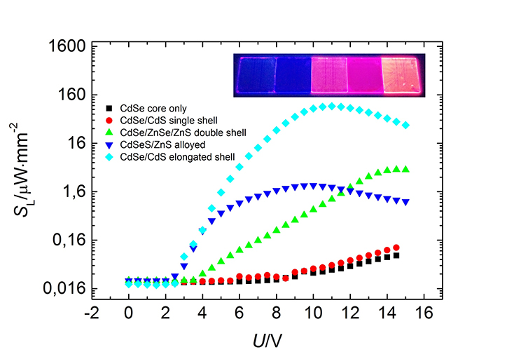
Figure 2 shows the density of the illumination power as a function of the voltage for different QD-LED setups. These setups are produced in the same way, except for the QD-layer. These layers distinguish in the material of the shells of the QDs. The shells are epitaxial grown semiconductors around the QDs which passivate and confine the charge carriers in them. With this approach, the suitability of the different shells were investigated electrically and optically. It was shown that it is important to choose the right material of the shells as well as the right shape. Present results were obtained within the project “Quaspink” (Sächsische Aufbaubank, SAB No: 100111575).
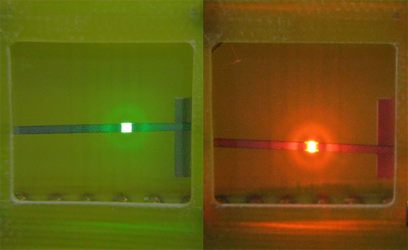
Within a project of the cluster of excellence “Merge Technologies for Multifunctional Lightweight Structures – MERGE” we participated to develop a method to integrate QD-LEDs on PET foils in lightweight structures. This could lead to two improvements. On the one hand, it could be possible to integrate luminous elements in every shape or color directly into lightweight structures during the production process. On the other hand, one of the biggest problems, the degradation of these QD-LEDs by external influences like water or oxygen, can be reduced. This would be a new approach for encapsulation and for the integration of such functionalities.
 Fraunhofer Institute for Electronic Nano Systems