 Fraunhofer Institute for Electronic Nano Systems
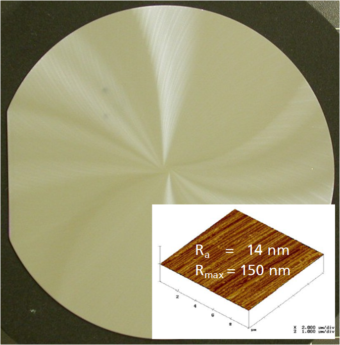
To further reduce the device thickness, the demand for wafer thinning has dramatically increased in recent years. With a thickness of less than 50 µm, the wafer becomes flexible and can facilitate new applications e.g. 3D interconnections of wafer stacks (Through-Silicon Vias, TSV).
New approaches for thin wafer handling in development
For the fabrication of ultra-thin wafers, temporary wafer bonding and debonding have been intensively developed to ensure the mechanical stability of the wafer while reducing its thickness. The department System Packaging focuses on adhesive temporary wafer bonding technology, where a peel-off de bonding process enables the removal of the device from the carrier wafer at room temperature after wafer thinning.
Adhesive wafer bonding
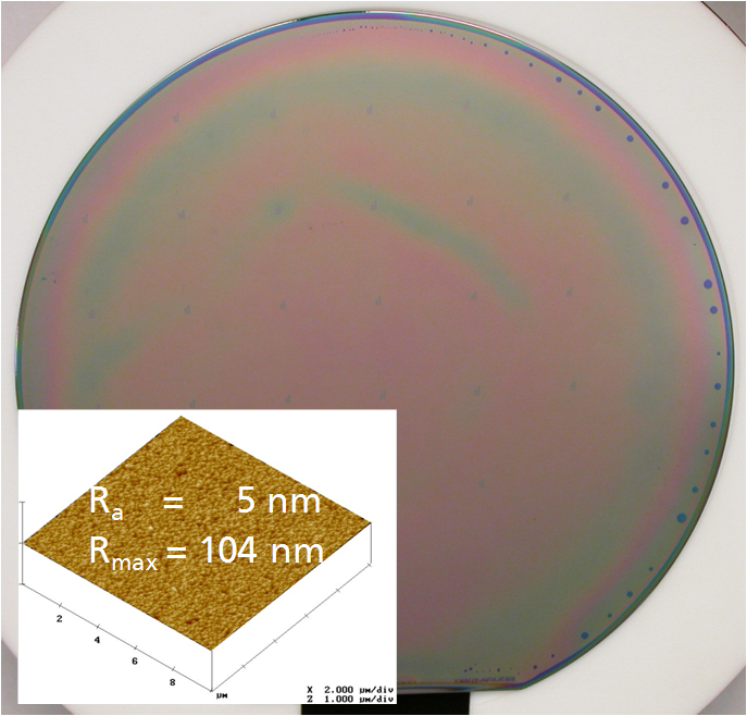
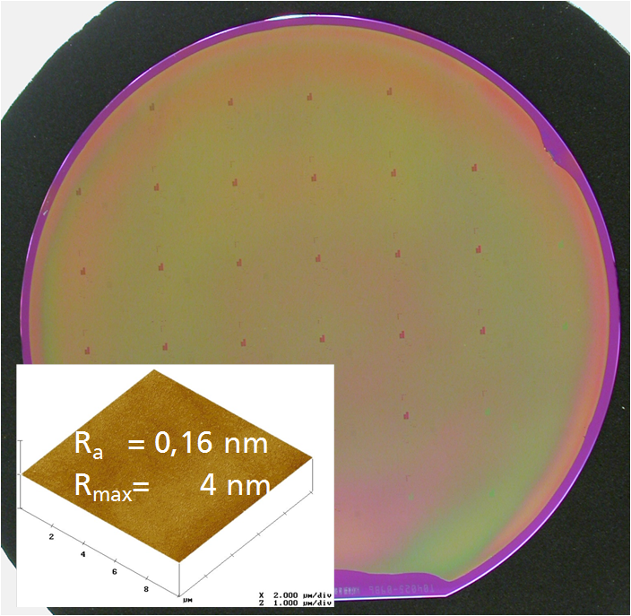
The complete process flow consists of an adhesive wafer bonding process of a carrier to a device wafer (temporary wafer bonding). The special carrier stabilizes the device wafer during the wafer thinning. Afterwards, the device will be rough (200-300µm/min) and fine (1- 10 µm/min) back grinded with high velocity. The rough and fine grinding generate defects in the material, reduce the mechanical stability and leads to wafer bending. After grinding, the surface roughness is less than 20nm. The damaged layer required a wet chemical or plasma dry etching process to reduce the defects and increase the mechanical stability. The modified surface roughness after etching is less than 10nm and can be minimized up to 1nm with chemical mechanical polishing. Finally, the carrier wafer will be removed with special thin wafer handling methods to avoid the cracking of the thin wafer (debonding).