 Fraunhofer Institute for Electronic Nano Systems
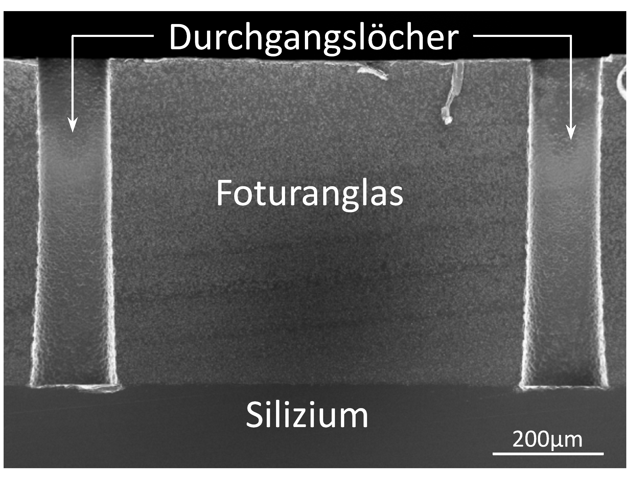
The surface roughness becomes very important when joining two substrates without an intermediate layer. While small variations in the surface roughness can be easily compensated by thick intermediate layers such as glass paste or epoxy resins, the atomic contact is crucial to form a strong and stable bond based on techniques without intermediate layers. For instance, anodic bonding is carried out with a surface roughness Ra below 1 nm. Other technologies require special pretreatments, like plasma activation with special gases or a wet chemical treatment, in order to create a smooth hydrophilic or hydrophobic surface.
In addition to a wet-chemical pretreatment of the wafers, a chemical-reactive plasma discharge prior to bonding increases the mechanical strength of a direct-bonded stack. The plasma activation can be applied to the whole substrate or limited to small areas and structures on the wafer. Even at annealing temperatures of less than 200 °C, the resulting bonding strength is comparable to those bonded at high temperature. Plasma pretreatment followed by low-temperature bonding can be used for joining material with different coefficients of thermal expansion. Therefore, it enables the integration of new and heterogeneous materials such as stainless steel or glass which is not anodically bondable.
Advantages of this bonding technology:
■ Short bonding time
■ High bonding strength
■ No additional intermediate layer
■ Independent on bonding environment, such as vacuum and nitrogen