Electromagnetic Near-Field Measurement Techniques


The More-Moore and More-than-Moore assembly trend of smart low-power electronic systems make the components become continuously smaller integrating heterogeneous functionalities with smaller switching times and therefore reduced energy consumption. In parallel, the signal-to-noise ratio decreases, making every new generation of a circuit more sensitive. For the developers of electronic circuits this results in increasing electromagnetic compatibility issues. Not only the electronic device itself needs to be protected but progressively each individual component on the printed circuit board must be considered. These boundary conditions require a focus on the parasitic influences during the system design to guarantee a flawless design. By using appropriate EDA tools and simulators, it is possible to analyze a multitude of such parameters in the design phase. However this does not allow for sufficient security, since the ratio between the biggest dimension (PCB) and the smallest structure (bond wire) can differ by several orders of magnitude and leads to extremely complex 3D models. Indeed, the radiating characteristics are directly determined by the switching behavior of the circuit and its geometric structure. Moreover, the internal signal level and the internal signal form of integrated circuits are not known and therefore assumptions have to be made.
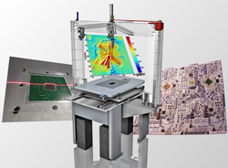
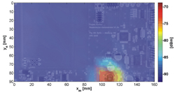
Near-field measurement technique provides a mitigation to this problem. They allow the precise detection of weak electric and magnetic fields within a resolution of a hundredth of a millimeter and can be employed for the characterization and discrimination of potential electromagnetic interference (EMI) sources in active systems. This measurement technology has the ability not only to locate EMI sources locally but also spectrally. Thanks to this dual property, it is possible to quickly and directly identify and correct conception faults at early design stages. However, near-field measurement systems need to be adjusted to the specific requirements of EMC compliance measurements. For these adjustments, the department research focuses on the influence of the near-field probe on the field to be analyzed itself and has developed methodologies to compensate this influence.
Such compensation is necessary, since a real probe is not only sensitive to the desired field component (i.e. the normal component of the E-field) but also on other field components such as the tangential E- and H-fields. A central research point of the department SWS related to this issue is the continuous improvement of the mechanical and electronic components of the near-field scanning system.
Beside the application field of EMC, the high and wide-band sensitivity of the developed near-field measurement technology allows the electromagnetic analysis of security-relevant systems such as smart cards, which is a new and promising application area of this advanced measurement system. By using near-field measurement methods it is possible to uncover weaknesses in such systems and elaborate countermeasure strategies.
 Fraunhofer Institute for Electronic Nano Systems