New characterization opportunities for surface processing


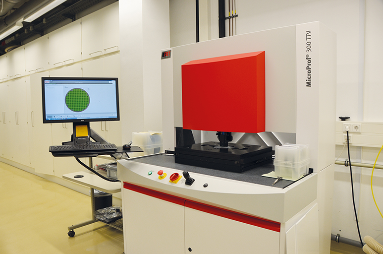
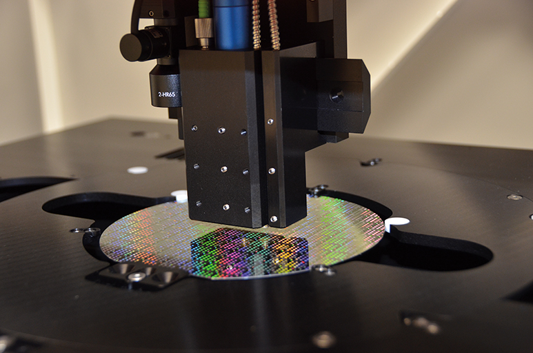
Surface processing, such as grinding or Chemical Mechanical Polishing, has become a basic technology in all areas of semiconductor processing. Both, More Moore and More than Moore applications, generate continuously increasing demands to the quality of these processes. In order to meet these requirements, a precise and reliable surface and substrate inspection is mandatory. The »UnitSC4see« inspection system allows a particle and defect detection even below 100 nm (app. 60 nm lower detection limit) by an innovative scattering light module. The additional 2D/3D brightfield module detects pattern defects, i.e. after CMP, based on microscopical image recognition. An additional »FRT MicroProf300TTV« multi-sensor measurement systems allows a comprehensive substrate characterization (TTV, bow, warp, …) using chromatic withe light sensors. The thickness of transparent films can be measured using a white light reflectometer. At least, an infrared interference sensor is able to measure membranes, cavities, and even stacked assemblies.
 Fraunhofer Institute for Electronic Nano Systems