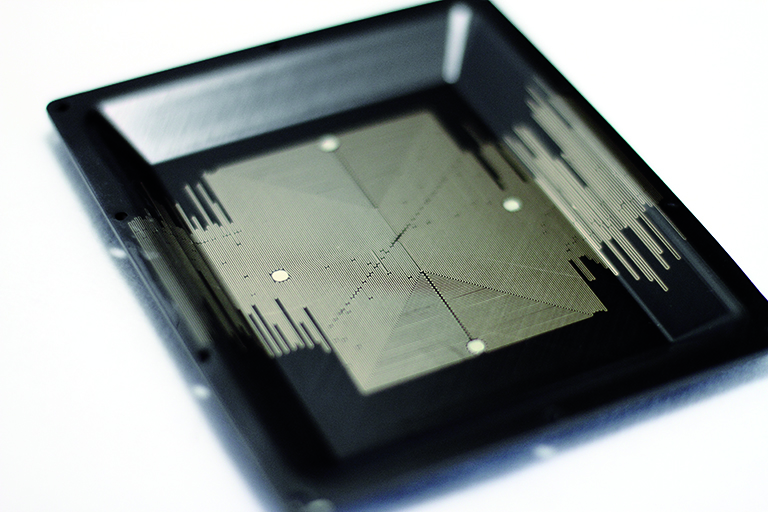
Tamper respondent envelope solutions realized by additive manufacturing – smart packaging solutions for secure applications
The UNSETH project aims to develop and qualify European-based packaging and assembly technologies applicable to both electronic modules and systems-in-package, compatible with low cost secure solutions, tamper detection features and higher tamper resistance.
Security has become a vital part of European electronic products and equipments as they handle sensitive data in uncontrolled environments and they face more and more IPR protection issues, counterfeiting and cloning issues. New applications combine a challenging set of requirements including low-cost, security and tamper-resistance. To meet the challenging requirements, Fraunhofer ENAS explores new hardware envelope solutions realized by three dimensional conformal conductive multilayer stacks upon non planar packaging parts. Furthermore, 3D embedded devices and active electronic mesh solutions within PCBs are realized by AT&S Austria Technologie & Systemtechnik AG using secure SiP components with active anti-tamper sensors from NANIUM S.A. as well as the combination of all, focusing on both the electronic modules themself as well as the manufacturing process. For the advanced technologies developed in the project, Thales Global Services brings applications for security and checks manufacturability of the technologies. Epoche and Espri S.L.U. is the security evaluation center and proposes a related protection profile. Fraunhofer ENAS evaluates the reliability of the smart envelope and develops prediction capabilities for life limiting failure mechanisms in the design of the security devices.
Together with partners, Fraunhofer ENAS is developing one module of a new security tool box which can be obtained by introducing functionalized packages with three-dimensional conformal conductive multi-layer stack used as tamper resistant envelope. In the proposed method a polymer (parylene) thin film is used as an insulation layer between the conductive multilayers and the interconnect vias are opened by a fine-tuned laser ablation process. The entire process for conductive multilayer fabrication and via filling is performed by aerosol jet printing (AJP) technique. A test program based on high-temperature storage, thermal cycling and pull tests is followed to compare several configurations, whereas today the solution is capable to withstand several hundred temperature cycles in the range of - 55 °C / 125 °C and 1000 hours of thermal storage at 125 °C without significant influence toward the overall performance.
 Fraunhofer Institute for Electronic Nano Systems
