Cool PoD: printed 3D chip-2-board interconnects


The possibilities of the Aerosol Jet® deposition are promising regarding packaging issues for electronic products and micro-electromechanical systems. The direct and maskless deposition of metal-based nanoparticle inks for chip interconnects as well as the different material compatibilities within usual assembly processes could be developed within the R&D project CoolPod, a CoolSilicon project funded by SAB-Foerderbank.
Goal of the CoolPod project was the development of a sensor system including an inertial sensor, an ASIC and a special wake-up generator device for low power consumption while sleeping. Each chip had a different thickness which makes it difficult to connect the components to the board by printing. Here, printing of interconnects could be used as an alternative to conventional wire bonding in terms of enhancing the degree of 3D system integration with synergies in reduction of size and of material consumption.
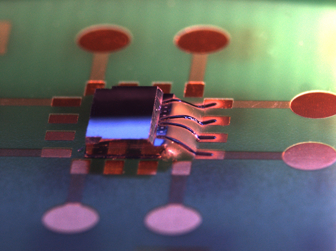
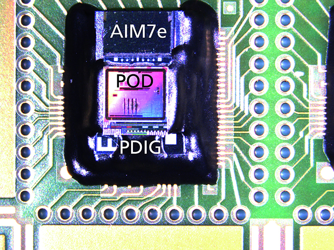
The stacked assembly “CoolPod” consisting of power down interrupt generator (PDIG), AIM-7e acceleration sensor (AIM7e) and ASIC was accomplished on top of a customized PCB by Microelectronic Packaging Dresden GmbH (MPD), Germany. The all over height of fabricated stack was measured with 3.8 mm whereas the footprint was identified with an area of 90 mm x 100 mm. The device itself is capable to wake up electronic microsystems from so-called power down mode due to mechanical impacts from environment using a self-generated energy impulse. Thereby energy could be saved significantly in comparison to existing solutions. The involved single chips are assembled manually and group-wise whereby stacking was established by depositing underfiller material between devices and PCB manually. Dam material was supposed to generate smooth topographic transitions between contact coordinates of each single device for better printing results between contact coordinates of each single device. Stacked assemblies were separated using dicing technology after fabrication due to handling reasons during printing. The center to center distance between two neighbored contacts of the ASIC were designed with a width of approximately 75 µm whereby one single contact pad is designed with a width of 50 µm what requires printed line widths for interconnects of 25 µm. A detailed view of a single stacked device is shown in figure 1.
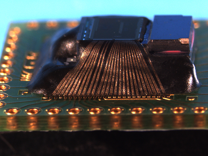
To reduce the problems of insufficient aerodynamic focusing due to high standoff distances the stacked device was inclined by 17.5° in reference to platen holder. This inclined position effectively decreases the overall distance standoff height between print-head and topography that has to be printed. Additionally the inhomogeneous topography of dam material leads to another inconsistency in terms of constant standoff height. Here in between neighbored printed interconnects at comparable level of height clearly strong differences in aerodynamic focusing are visible. The effort of performing such a kind of printing process however is time consuming, as the PCB has to be rotated according to the considered contacts that have to be printed sidewise. Also connecting of multiple stacked devices onto one extensive and inclined substrate is only possible in a limited manner at the given process setup because of possible collisions between printhead and substrate. In figure 2, one completely contacted sample of CoolPod is exemplarily shown.
Aerosol Jet printing was successfully evaluated as key enabling material transfer technology in the field of alternative approaches for 3D integration with systems from the field MEMS / NEMS packaging. With stacking of single devices, savings in footprint and volume could be achieved.
In parallel this developed packaging technology could be used for several other applications which would lead to additional innovations in the field of micro technology and electrical interconnects over 3D topographies.
Acknowledgment
Partners of the project were: Electronic Design Chemnitz GmbH, Microelectronic Packaging Dresden GmbH and TU Chemnitz. The work related to integration technologies of single and stacked components on PCB was partly supported by the European Union (EFRE) and by the Free State of Saxony, Germany, within the research project CoolPod funded by SAB-Foerderbank (100107775).
 Fraunhofer Institute for Electronic Nano Systems

