Characterization of Copper Alloys for Self-Forming Barriers
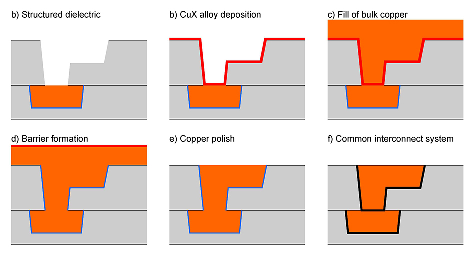
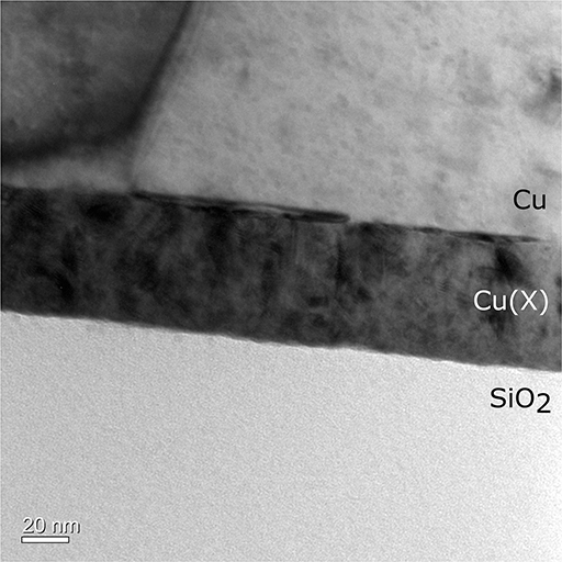
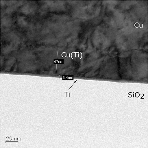
Self-forming barriers (SFB) are used in copper interconnect systems and offer the advantage of ultra-thin barrier layers, which provide resilience against the diffusion of copper into the oxide. At Fraunhofer ENAS, various copper alloys can be deposited to form a stable barrier at the interface to e.g. the silicon dioxide, typically requiring a temperature treatment for the activation, too. These systems include Cu alloys with Mn or Ti, each forming a Mn or Ti containing barrier.
The characterization of the SFB is usually done via triangular voltage sweep. This method analyzes the barrier stability and measures the copper ion drift within the dielectric material. The thickness and quality of the barrier layer can be analyzed with scanning electron microscopy after focused ion beam (FIB) cuts, for example.
 Fraunhofer Institute for Electronic Nano Systems

