Power packaging – silver and copper/tin sintering for power electronics
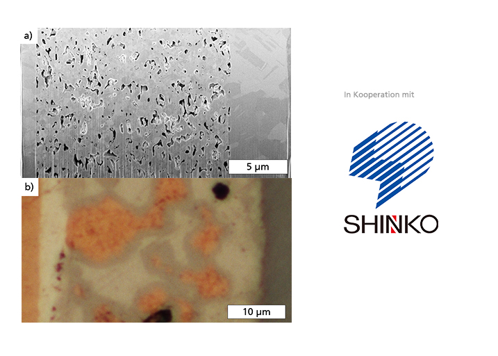
The market for power packaging grows about 8 percent per year. Higher power densities, needs for lower costs, reliability and a higher grade of integration demand for new packaging concepts and materials. One critical point is the die attachment, which can lead to premature failing of a power module. Fraunhofer ENAS investigated silver sintering materials but also transient liquid phase (TLP)-based pastes for die attach within a research and development project together with SHINKO (Japan). To get optimum process parameters, a parameter screening is done for the die attach material. Printing parameters, drying conditions and the bond process have to be considered. In general, the bonding parameters have the highest influence. It is necessary to keep the bonding temperature low to not crack the samples due to CTE mismatch. Examples of the resulting interface are shown in the bottom figures (a and b). The samples were tested in a power cycling test afterward. Usually, failures could be classified into two main physical failures: Die attach or wire bond failure. So far, the results show that wire bond failures dominate the die attach failures for both die attach materials, pointing to high reliability of the module.
 Fraunhofer Institute for Electronic Nano Systems