Profile optimization of multilayer PCBs in simulation and deformation measurements
Today’s electronics developments are driven by an increase of functional density but also by increasing the reliability of all components on chip, package and board-level. Thereby, the interconnection to the board is one key issue for the system reliability and the mechanical behavior of mounted or embedded components, and the board behavior has to be well understood and represented in terms of thermo-mechanically induced stresses and strains. Therefore, a detailed representation of printed circuit board (PCB) by means of finite element method (FEM) was established. The modeling approach for considering multilayer PCBs based on the commercial software ABAQUS has been verified by experimental warpage measurements, performed by using the MicroProf 300 test equipment.
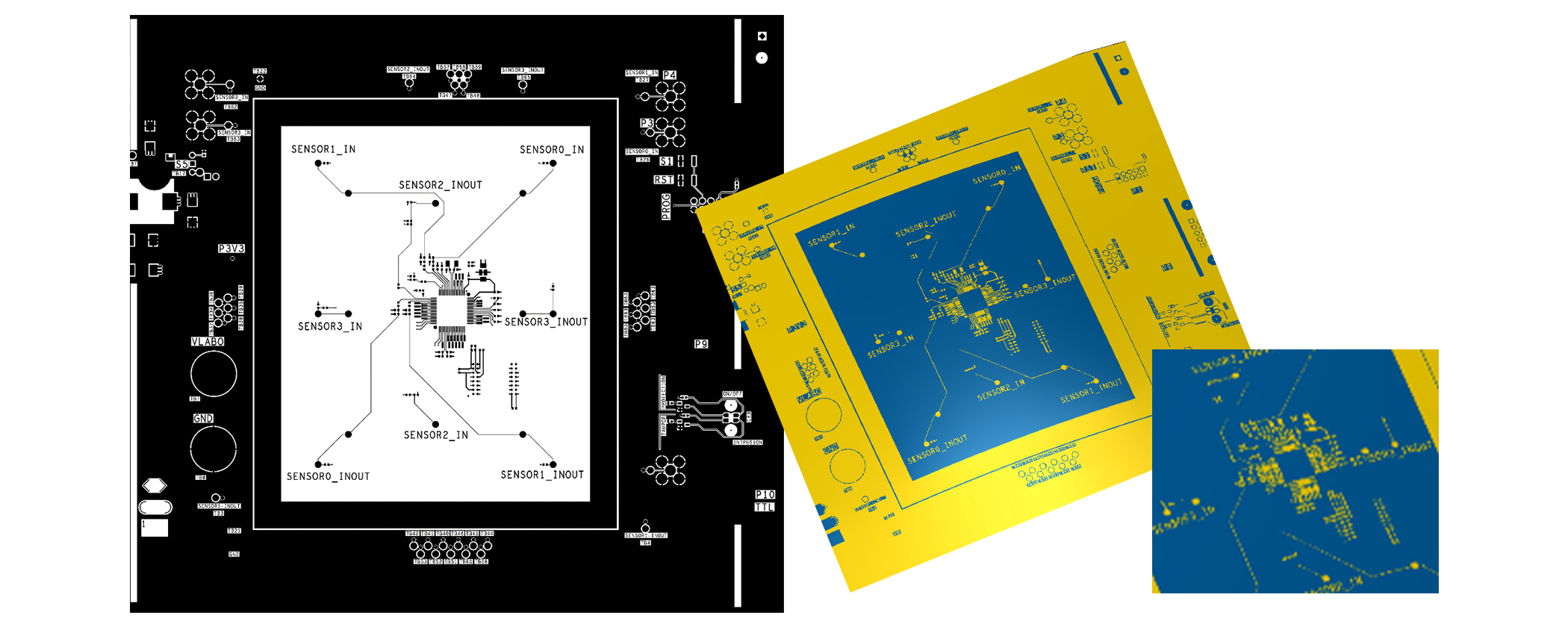
A Python V2.7.3 based user routine is now able to adequately represent multilayer PCBs within ABAQUS. The procedure uses images of each layer layout and its thickness as input for discretization into a user defined rectangular mesh (source grid). After buildup of a CAE-model (ABAQUS GUI), considering drills and cut-outs and meshing of the model with user defined in- and out-of-plane mesh density, elements of the finite elements model are mapped onto the corresponding segments of the image discretization to assign the material information to the finite elements model. The advantage is simple meshing of the complex base geometry and high accuracy in detail with appropriate finite elements discretization, keeping the ability of using a wide range of material properties for the model such as linear elastic, elastic-plastic or visco-elastic behavior. Simulation is now and in the future able to describe the thermo-mechanical behavior of loaded PCBs, based on a more precise multilayer PCB representation, regarding the interaction with surface mounted as well as embedded devices.
 Fraunhofer Institute for Electronic Nano Systems