KoliBriS – Modular technology platform for highly compact inertial sensors with integrated circuit electronics
The name KoliBriS stands for »Compact Low-Power Wideband Sensors with Integrated Circuit Electronics«. KoliBriS is a research and development project led by EDC Electronic Design Chemnitz GmbH and carried out with the cooperative participation of the industrial partner X-FAB MEMS Foundry GmbH and the research partner Fraunhofer Institute for Electronic Nano Systems ENAS in the period from August 1, 2016 to October 31, 2019. The project is supported by the BMBF.
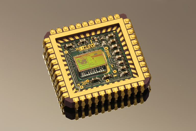
For optimal interaction between mechanics and electronics, it is important to consider these systems as one unit. Because of this, MEMS and ASIC are co-designed and mutually adjusted in an iterative development process. Hereby, the technological boundary conditions of the selected fabrication technologies play an important role, and their design rules are important for the dimensioning of the MEMS.
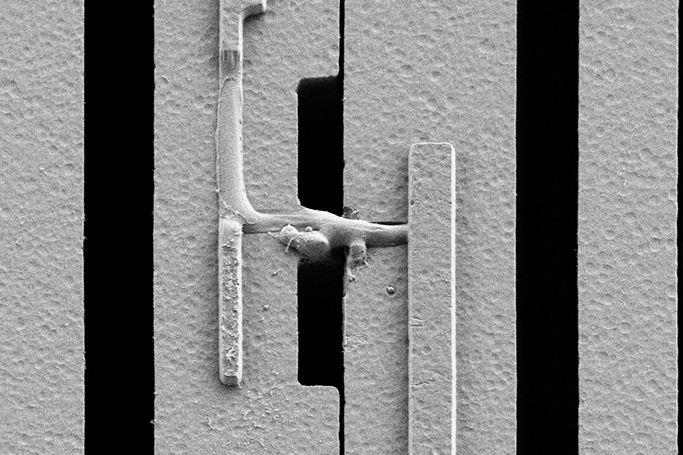
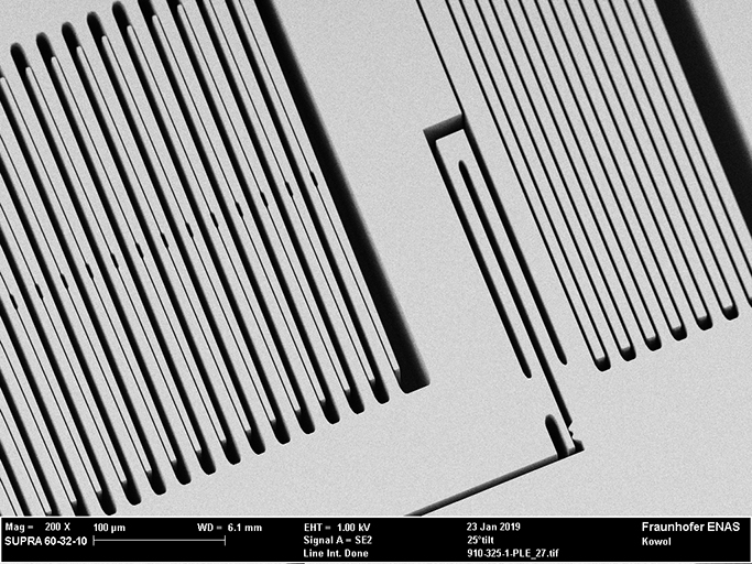
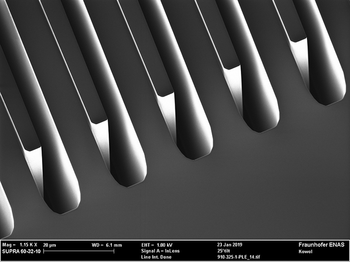
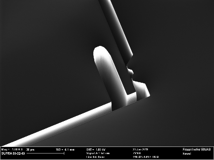
Various inertial sensors were developed within the three-year project period. This includes an uniaxial acceleration sensor up to 1.5 g with a signal bandwidth from 100 Hz to 8500 Hz. The design of this sensor was created at Fraunhofer ENAS, simulated using finite element methods and converted into a layout. For its implementation, the X-FAB further developed its MEMS technology to achieve structure heights of 75 µm. Using a »post process gap reduction« technology, the 3 µm wide etched initial gaps are reduced to 500 nm and are firmly bonded and fixed in this position at suitable points by micro-welding in order to significantly increase the capacitive sensitivity. This process was developed, investigated and characterized at Fraunhofer ENAS and then transferred to the project partner EDC. The current consumption of the sensor system (micromechanics and integrated electronics) is 500 µA during operation and this sensor is suitable for the detection of the smallest vibrations.
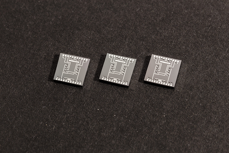
Due to the requirement for an application for pump monitoring by an associated partner, an additional acceleration sensor with a range of ± 20 g was also included in the project and developed. The MEMS is designed for the BDRIE (Bonding and Deep Reactive Ion Etching) technology established at Fraunhofer ENAS in the glass-Si-glass variant. In parallel to the KoliBriS project and in connection with the implementation of a new wafer stepper, a new technology idea was developed between 2017 and 2018 and has now been patented (DE102018210810B3). The capacitive gaps with typical values of 1.8 µm are reduced down to the sub-µm range while maintaining the aspect ratio that can be achieved using etching technology. The created MEMS design, the process development and adaptation of the etching process for the small gaps as well as the fabrication of this 20 g acceleration sensor demonstrate a first successful implementation of this idea.
The third sensor system is a gyroscope for the detection of angular rate or angular speed. The objectives in the KoliBriS project were to increase sensitivity and improve thermal stability with regard to the drift of the sensor, and the size reduction of the electrical through contacts in the silicon chip. The former target is achieved by increasing the structure height from typically 50 µm to 60 µm or 70 µm while maintaining the typical width of the etched capacitive gaps (1.8 µm). For the latter two goals, the BDRIE technology as a full silicon technology variant was further developed in the project, and adequate, optimized sensor designs were created.
Working prototypes for all sensor systems show the great potential of these three innovations to increase the sensitivity of capacitive sensors.
 Fraunhofer Institute for Electronic Nano Systems