Technology development for analog high-frequency CNT FETs


Within the Cluster of Excellence “Center for advancing electronics Dresden (cfaed)“ the Carbon Nano Devices group at the Center for Microtechnologies and Fraunhofer ENAS develops the technology for analog field-effect transistors (FETs) based on carbon nanotubes (CNTs). Applying a dielectrophoretic approach, arrays with individually addressable FETs were prepared using standard silicon technology on 150 mm wafers, thus enabaling statistic evaluation of different aspects of CNT transistor fabrication.
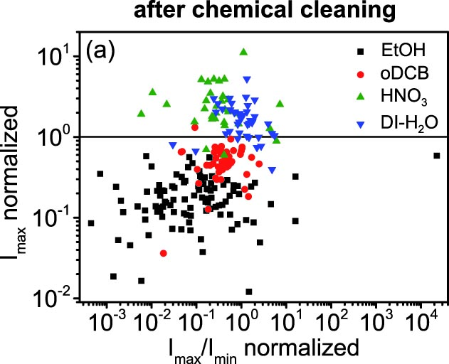
Since dielectrophoresis is a liquid-based technique where surfactants are involved to maintain a stable dispersion, it is of crucial importance to examine their influence on electrical properties of FETs. Considering that surfactant molecules are potential charge-traps, four different approaches for cleaning of FETs were investigated by means of statistical studies on more than 600 CNT-FETs. From combined XPS, Raman spectroscopy, and electrical studies it turned out that especially DI-H2O and HNO3 treatment appeared to be most effective for removal of surfactant residuals. Thereby, especially HNO3 treatment significantly improved the on-current as well. Equally, there was a significant influence of a subsequent annealing treatment apparent which significantly affects hysteresis behavior and reduces the device-to-device variance.
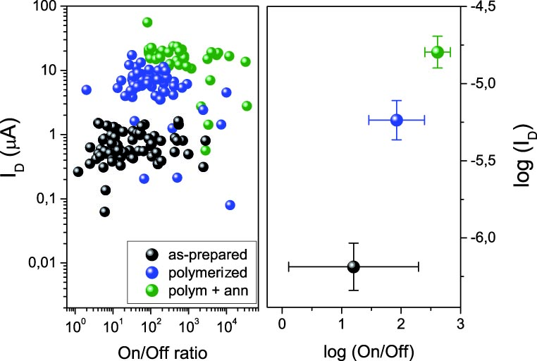
Beside the presence of surfactants, CNTs can agglomerate into bundles during the assembly. This could lower the maximal current and reduce the transistor operation frequency. Therefore, alternative approaches toward enhancing the individualization of nanotubes by polymerization after integration were investigated and shall represent a milestone in improving the FET characteristics. We used a styrene-sulfonic acid sodium salt (NaSS) in the so-called self-initiated photografting and photopolymerization (SIPGP) process. We report improved device-to-device consistency, lower variability in the threshold voltage (Vth), higher on/off ratios and drain currents (see Fig. 2). Moreover, subsequent vacuum annealing was found to induce ambipolar behavior, which could be conserved upon long-term storage under ambient conditions.
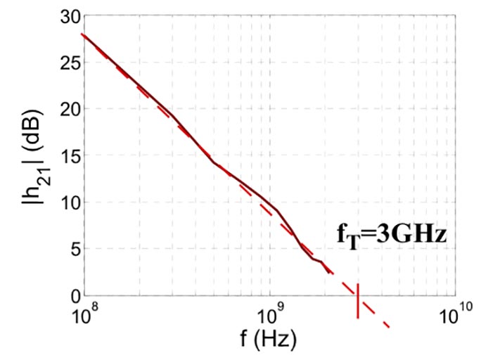
Furthermore, FETs in a special high-frequency layout were fabricated on 6 inch wafers. To minimize parasitic capacitances a local and embedded bottom gate has been realized by damascene technology. A large amount of parallel aligned CNTs has been assembled on comb electrode structures to enable high transistor currents which are required at high-frequency operation. Extended electrical characterization on the first HF-FET generations, which used 50 nm SiO2 gate dielectric and 0.8 µm channel length, operated already at a transit frequency of up to 3 GHz (Fig. 3). Ongoing work is focusing on higher device performance by shrinkage of device dimensions, integration of high-k gate dielectrics and technology optimization.
 Fraunhofer Institute for Electronic Nano Systems