 Fraunhofer Institute for Electronic Nano Systems
Technology platform for Carbon Nanotube devices

Carbon Nanotubes (CNTs) are considered as an emerging functional element in advanced electronics and sensors seeking for new functionalities, further miniaturization and alternative device technologies. In a close cooperation between Fraunhofer ENAS and the Center for Microtechnologies at Chemnitz University of Technology, a nanotechnology platform was established enabling manufacturing of CNT-based nanodevices compatible with wafer-level silicon technologies.
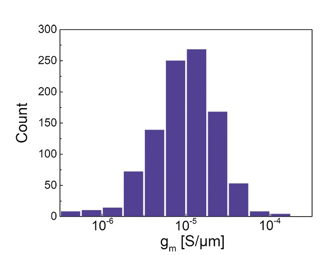
A flexible prototyping technology was developed for CNT-based field effect transistor (FET) arrays on wafers up to 200 mm diameter. Based on this, various applications can directly be build on optical, chemical, biological or mechanical strain sensors. So far the fabrication yield is above 90 % with respect to FET on/off ratio of larger than 1000. A flexible design and reliable fabrication process allows to provide specific FET geometries with channel length down to 300 nm, high device density and low device variability (Fig. 1).
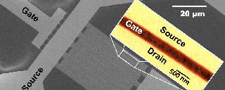
High-performance FETs were realized by addressing applications in analog high-frequency (RF) front-end transceiver electronics. Therefore, a new class of FETs are under development perusing for higher energy efficiency and transmission bandwidth. Using a multi-layered nanostructuring approach on wafer-level, complex device structures were developed by implementing asymmetric FET geometries with 280 nm channel length (Fig. 2). Thereby, realizing an extrinsic operation frequency of up to 14 GHz.
On a system level, we developed heterogeneous wafer-level technologies for the integration of CNT devices in MEMS, MOEMS or ASICs.