Fraunhofer Institute for Electronic Nano Systems
Simulation of Devices, Processes and Equipment
The department Nano Device Technologies has many years of experience in simulation and modeling of processes and equipment for the semiconductor industry.
As the development of new technologies requires new or optimized processes and equipment, advanced models and simulation tools are specifically designed for PVD, CVD, ALD as well as CMP. They support the development of improved deposition and polishing techniques by optimization of process conditions, tool configuration, and feature topography.
The simulation of PVD processes has been extensively applied to study the formation of ultra-thin metal layers as diffusion barriers for adjoining copper interconnects, as contact layers, or as seed layers for subsequent deposition steps. PVD simulations are able to cover all important aspects of the deposition such as rate, conformity, composition, or energy deposition even for the demanding conditions within small vias or trenches. CVD simulation applies hydrodynamic methods at the reactor scale and ballistic methods at the feature scale. In addition to optimum deposition rates, the uniformity of film thickness and doping across large wafers and batch sizes, as well as conformal film deposition in deep trenches and vias are predicted and optimized.
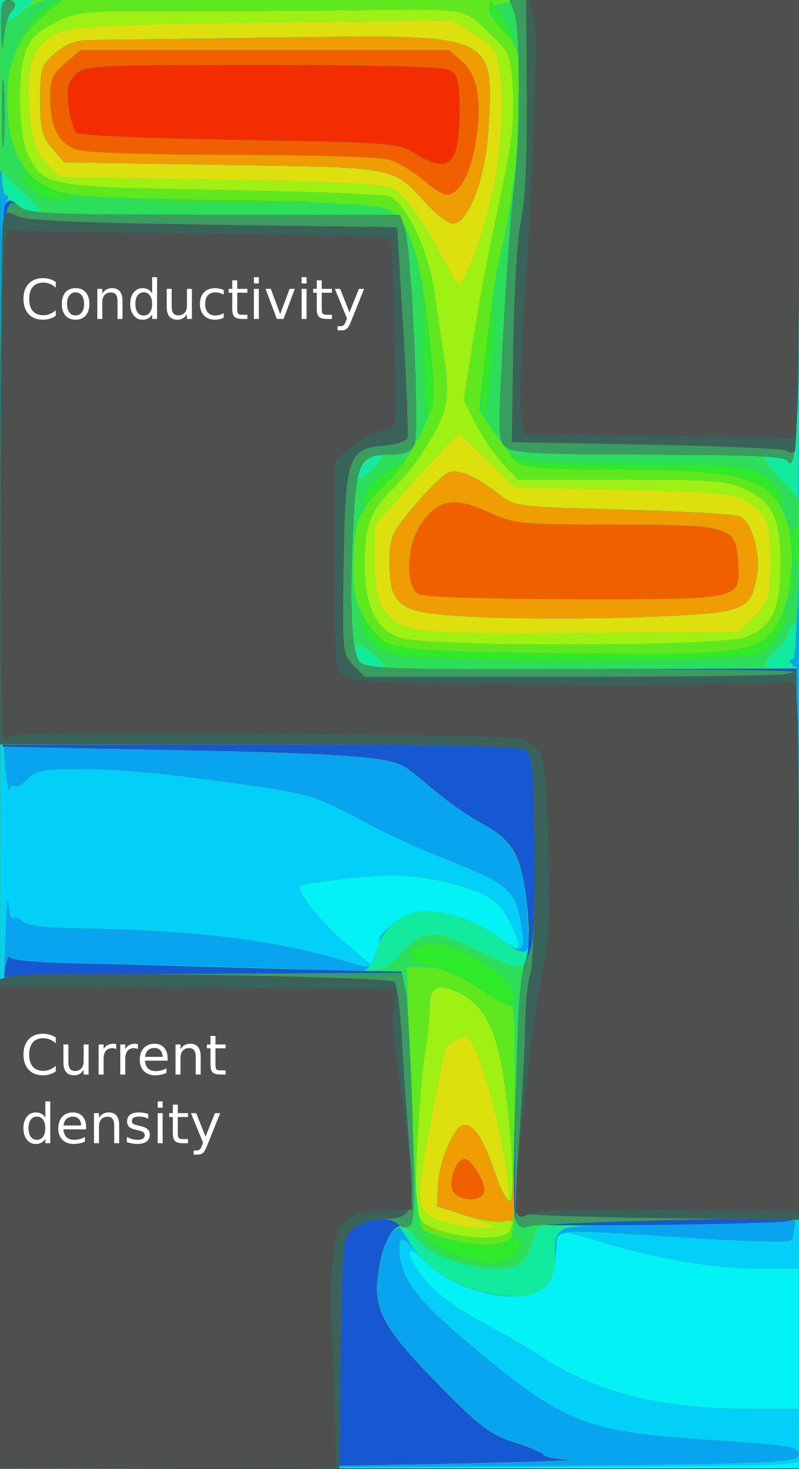
An emerging field is the device simulation which becomes more and more important for understanding device behavior and optimizing device performance. Using adequate models, the increase of transistor performance induced by stressor films prior to metallization can be predicted. Device simulations are also applied to model the electrical as well as the heat transport within nanoscale interconnects. Besides microelectronics applications, device simulations are also applied to study the influence of novel solar cell concepts on cell efficiency.
Simulation and modeling of the electrical reliability is another key issue on the way to a comprehensive description of the interconnect system. Biased temperature stress (BTS) data from inter-metal dielectrics can be analyzed and compared with various available models in order to investigate the electrical failure mechanisms.
For future nanoelectronic and NEMS devices, modeling of materials properties at the nanoscale is becoming more and more important. Therefore, a new research area is the ab-initio simulation and modeling of transport properties of nanostructures, such as nanoscale Cu interconnects and carbon nanotubes. Furthermore, quantum chemical modeling and simulation supports the development of metal ALD processes.