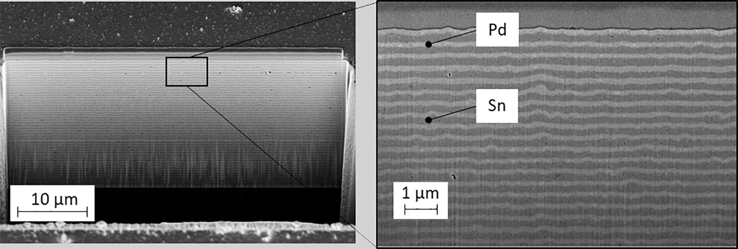
Electro chemical deposition of integrated reactive Pd/Sn multilayer systems


The reduction of process temperatures is essential for the integration of heterogeneous materials. For more than 10 years, Fraunhofer ENAS develops integrated reactive material systems (iRMS) as internal heat source for bonding applications on wafer, chip and component level. The energy stored in the reactive multilayer stacks is released upon ignition. The resulting self-propagating exothermic reaction generates the heat directly at the bonding interface. Within the public funded project ElisA, electroplated Pd/Sn multilayer system are being developed as an alternative to sputtered reactive systems. The electroplated multilayer system are deposited in a dual bath technology, enabling the stacking of reactive multilayers directly on standard substrates such as silicon and glass as well as printed circuit boards and ceramic substrates. The reactive layers grow directly on the printed base metallization of the printed circuit boards or ceramics. The thickness of the reactive multilayers varies between 20 µm and 50 µm depending on the substrate and premetallization. Applying a local ignition impulse (short electric spark), the exothermic reaction in the Pd/Sn multilayer stack propagates with a maximum velocity of 5.7 m/s and the metallization of the bond partners melt. The bonding technology enables the encapsulation of temperature-sensitive components without external heat input within fractions of a second. It can be applied for printed circuit boards as well as ceramics. Even pre-assembled components on the printed circuit boards are not affected by any subsequent thermal load.
 Fraunhofer Institute for Electronic Nano Systems