
Introduction
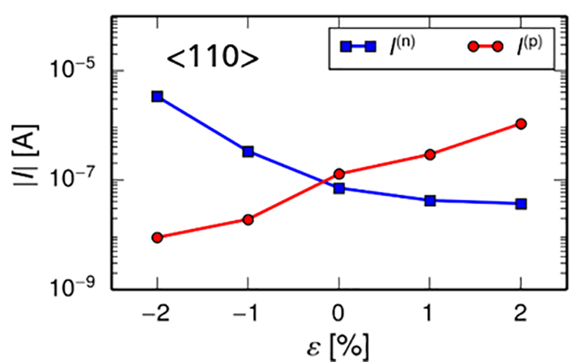
Straining the silicon in the channel of ULSI transistors is one of the key enabling technologies for increasing the performance of modern processors while simultaneously reducing its power consumption. Usually several stressor technologies such as strained nitride liners or SiGe pockets are combined to achieve the desired stress levels in the transistor channel. In the present work we focus on strained nitride liners and how their performance is influenced by the formation of the source/drain contacts. Contact formation requires opening of the stressor film which will lead to a partial stress release. In addition, a strained contact metallization will act as an additional stressor on the transistor channel. An analysis of the actual strain state in the transistor channel of ULSI devices by analytical techniques is very demanding and still far from routine use. Thus, to date simulation is the only mean to study and optimize the function of the various stressors. Usually two-dimensional models are convenient for the modeling of stress transfer from a stressor to the channel. However, if source/drain contacts are present three-dimensional models are required due to the small dimensions of the contacts. In general, three-dimensional simulation models are very demanding with respect to simulation time as well as to memory requirements. Thus a careful model design and optimization is required.
Transistor model
The flexible three-dimensional model described in this report was developed within the CoolTrans project together with GLOBALFOUNDRIES and Chemnitz University of Technology. Within that project, a comparison of the stressor performance between different technology nodes including several technology options was indented. Thus a highly flexible and adaptive model is required. In a first step, a number of important technology parameters and dimensions have been identified. Based on these, a parameterized two-dimensional transistor model was built. All dimensions have been chosen in such a way that the models cross sections are as close as possible to real device cross sections measured by electron microscopy. For robustness, the basis model of the transistor including the gate contact and spacer was constructed based on simple geometric elements using SYNOPSYS SENTAURUS Structure Editor.
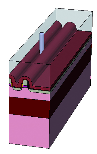
The basic geometric model can now be used in a second simulation step which is a process simulation step. Using SYNOPSYS SENTAURUS Process, we were able to simulate the deposition of the nitride liner while simultaneously the stress in the growing film is considered solving the equations of thermomechanics. Depending on the type of stress in the film (tensile or compressive) and how the stress is created, slightly different simulation strategies are required. In a similar way, further process steps such as TEOS oxide growth, contact hole formation and contact metallization are added. In this stage, the model is still two- imensional and all objects including the contacts have an infinite width and can be considered as trench-like. Before the model is switched to a threedimensional one, a thorough optimization is performed in order to make the mesh, which is used for the numerical solution, as coarse as possible while conserving the required accuracy of the results. Calculations based on this model are now very fast and the memory requirements are low. Now, having a compact and robust model we can switch to three dimensions by modeling contacts with a finite width and a circular cross section. Again, SYNOPSYS SENTAURUS process is used for modeling the process steps including a strained contact metallization. By increasing the contact width to a very high value, the three-dimensional model can be compared to the two-dimensional one and indeed identical stress distributions are found in the channel for wide trench-like contacts which resemble the two-dimensional situation.
Performance and results
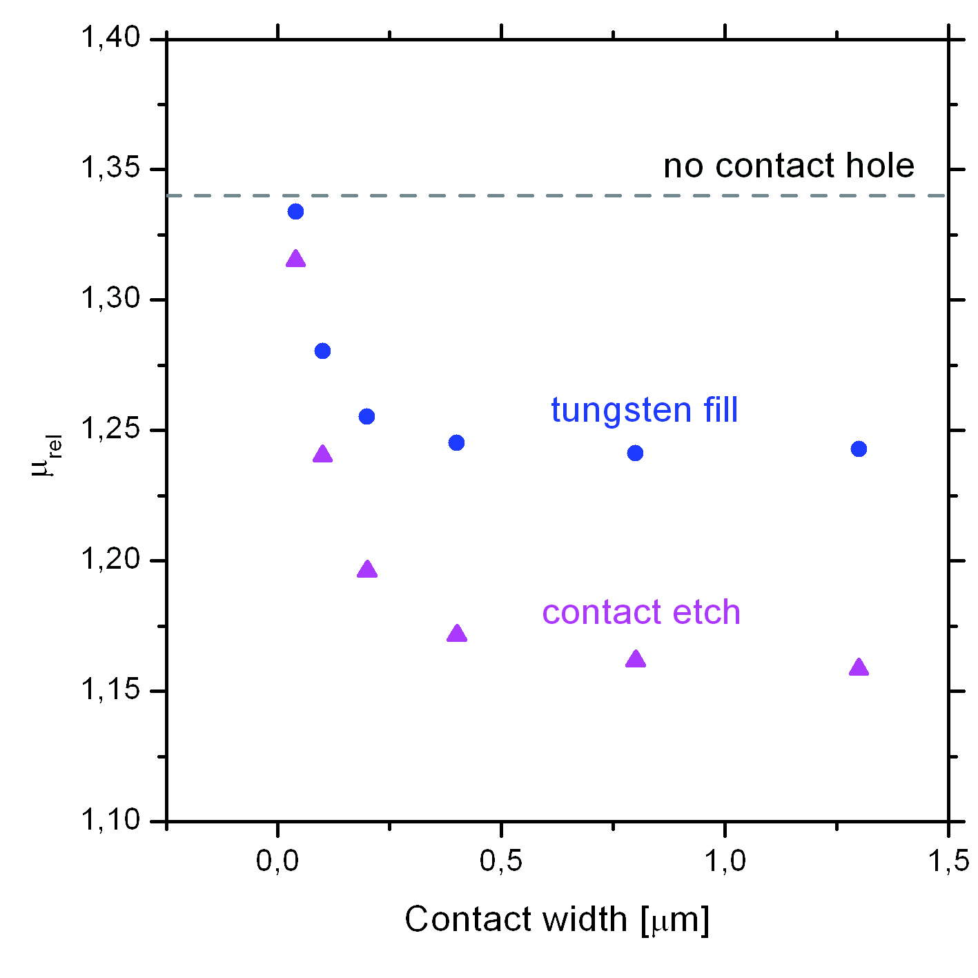
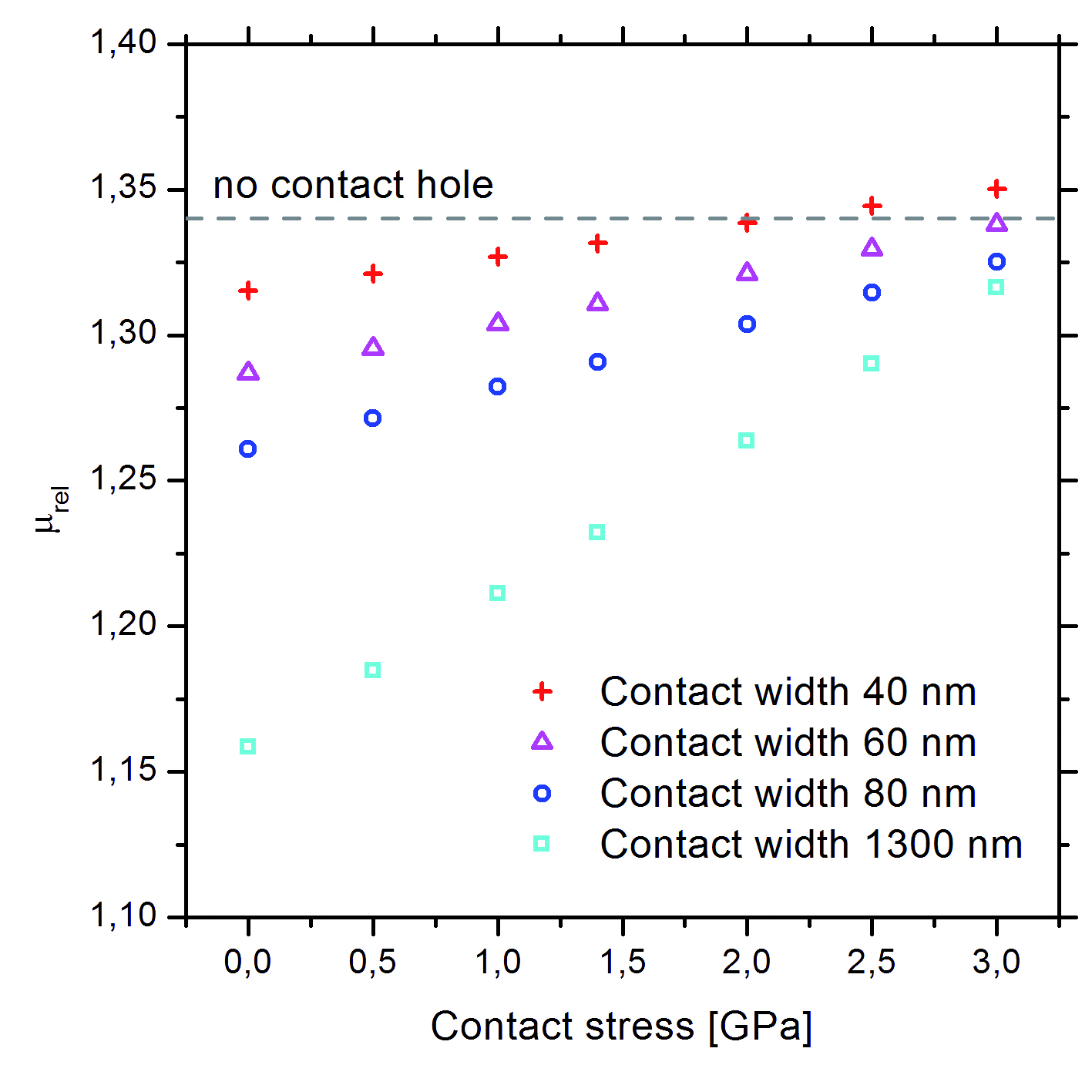
Based on the procedure described above a very robust and computationally efficient three- imensional parameterized model for ULSI transistors including strained source/drain contacts and strained nitride liners is now available at Fraunhofer ENAS. Due to the optimization of the model, the computer time required is on the order of several tens of minutes. Thus the model is suitable for extensive simulations including parameter variations and simulation based process and design optimization. Within the CoolTrans project the model was used for a detailed analysis of the interplay between strained nitride liners and contact metallization. It was found that the contact formation may have a drastic influence on the stress transfer from the nitride liner to the transistor channel. In case of very wide contacts, the performance gain due to the strained nitride liner is completely lost when the liner is opened for contact formation. This performance loss can be partially recovered by using high-stress tungsten in the contact. However, due to process limitations only tensile strain is available for the contact metals and thus only nMOS transistors having a tensile strained nitride liner will benefit from this performance recovery. In contrast, the pMOS which requires stress of the opposite sign for a performance gain (compressive nitride liner) will always be degraded by contact formation and no recovery is possible by a strained contact metallization. Details and further results of the study are summarized in an upcoming paper.
 Fraunhofer Institute for Electronic Nano Systems
