Simulation of TaN atomic layer deposition for copper diffusion barriers of 28 nm CMOS devices


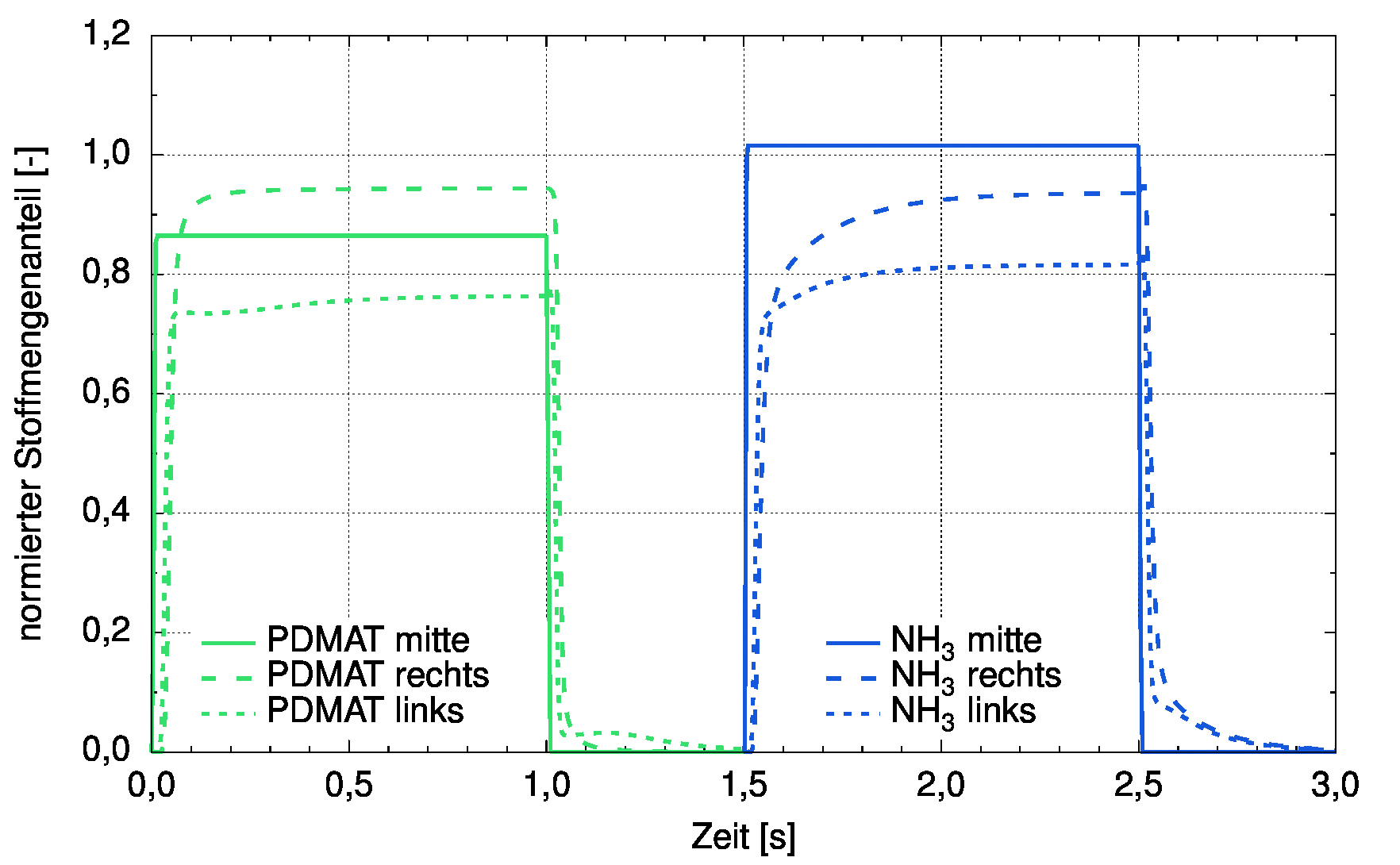
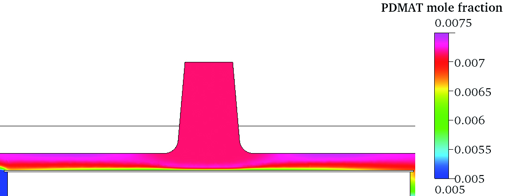
The progressing down-scaling of microelectronic devices leads to an increasing demand for deposition technologies which can produce uniform, homogeneous and ultrathin layers. Atomic layer deposition (ALD) has the capability to produce such layers even in features with high aspect ratio. In the EVOLVE project together with the chip manufacturer GLOBALFOUNDRIES, the Fraunhofer IPMS-CNT and the TU Dresden, we investigated a TaN ALD process for the manufacturing of copper diffusion barriers using reactor scale simulation. Using simulation, we were able to analyze the precursor distribution during dosing and purging steps in a top-injection single-wafer reactor. We experienced a reduced precursor concentration directly above the heated wafer in our simulation. A high temperature gradient is observed above the wafer due to the temperature difference between the hot wafer (200 °C) and the colder gas inlet (90 °C). Temperature gradients cause thermodiffusion, where the larger molecule (precursor) diffuses from the hot area (wafer) to the cold area. Using reactor scale simulation, we were able to get useful insights into the field of reactor flow and the precursor distribution, which would not be possible otherwise. Based on these findings, further process optimization steps will be performed.
 Fraunhofer Institute for Electronic Nano Systems