 Fraunhofer Institute for Electronic Nano Systems
Cleaning
| RCA clean |
| Piranha clean |
| DI-water flushing |

© Jürgen Lösel for cfaed, TU Chemnitz
© Fraunhofer ENAS
© Fraunhofer ENAS
© Fraunhofer ENAS
© Fraunhofer ENAS
© Fraunhofer ENAS
| RCA clean |
| Piranha clean |
| DI-water flushing |
| Thermal oxidation | dry, wet, HCl |
| Annealing | inert, reducing, oxidizing, ambient and forming gas |
| Diffusion | POCl3 |
| Sputtering | Ag, Al, Al-alloys, AlN, Au, Co, Cr, Cu, CuMn, CuTi, CuZr, Hf, Mo, Ni, NiMo, Si, Ta, TaN, Ti, TiN, TiO2, TiW, W, metallic glass, pyrex | |
| Ion beam sputter deposition | Al, Co, Cr, Cu, Mo, Ni, Ru, Ta | |
| Electron beam evaporation | Al, Co, Cu, Ni, Pd, Pt |
| Plasma enhanced CVD | PETEOS-SiO2, SATEOS-SiO2, Si3N4, SixOyNz, SiCH, SiCOH, black diamond, diamond-like carbon, CNTs | |
| Low-Pressure CVD | SiO2, Si3N4, polysilicon, amorphous silicon, SWCNT/MWCNT | |
| Metal-organic CVD | Cu, TiN | |
| CVD | Parylene N, C, D, F, AF4 |
| Metals | Ni, Co, Cu |
| Metal oxides and nitrides | Al2O3, CoxOy, CuxO, NiOx, TiO2, TaN, TiN |
| Electrochemical deposition (ECD) | Au, Cu, Ni, Pd, Sn, Au-Sn, Al (ionic liquids) | |
| Electroless deposition (ELD) | Au, Ni |
| Dielectrophoresis (DEP) | selective placement of nanomaterials (e. g. CNTs, nanowires |
| Spin-on | dielectrics, porous ULK |
| Electron beam lithography | resolution: < 50 nm |
| Projection lithography | 400 nm |
| Contact lithography | 2 µm |
| Nano imprint lithography | resolution: 50 nm |
| Spray coating | |
| Spin coating | |
| Plasma strip | oxidizing, reducing |
| Wet processes | ||
| Metals | Al, Au, Cr, Cu, Pt, Ti, W | |
| Non-metals | AlN, CuxO, Si3N4, SiO2, Si, polysilicon, glass | |
| Dry processes | ||
| Metals | Al, Cr, Cu, Ti, Ta, TiW, W | |
| Non-metals | Si, polysilicon, SiC, SiO2, Si3N4, silicides, TiN, resists, glass, low-k dielectrics | |
| Deep reactive ion etching | Si | |
| Lift-off | ||
| Gas phase etching of SiO2 | ||
| Assembly of CNTs |
| Thermal evaporation | Al, Ag, Ca, MoOx, HMTPD, CBP, TPD, mCP, ZnPc, C60, LiF, spiroMeOTAD |
| CMP for patterning | Al, Cu, Ge, Si, SiO2, W, barriers (TiN/Ti, TaN/Ta), ceramics (LiNbO3, LiTaO3), glass, isolators, stainless steel | |
| Planarization and surface finishing | ||
| Grinding | Si, glass, ceramics | |
| Spin etch | Si, glass | |
| Through silicon vias | ||
| Integration concepts | via last, via middle, vias for glass and silicon substrates | |
| Processes | deep etching, isolation, metallization, lithography in holes | |
| Metallization | metal-CVD, RDL, UBM, bumping (PVD, ECD, screen printing, aerosol jet printing) | |
| Wafer thinning and handling | Si, glass, ceramics | |
| Temporary wafer bonding and debonding for thin wafer handling | ||
| Hybrid and vertical integration of MEMS/NEMS | ||
| Aerosol jet printing | ||
| Biocompatible packaging (Parylene (C, D, F)) incl. pre-treatment (silanization) | ||
| High aspect ratio microstructures |
| Conventional, permanent wafer bonding | ||
| Silicon fusion bonding | RT ... 100 °C, 100 °C ... 200 °C, 200 °C ... 400 °C, > 400 °C, Si, borosilicate glass, foturan glass, quartz glass, LiTaO3, LTCC, stainless steel | |
| Anodic bonding | RT ... 550 °C, 0.... 500 kPa, 0 ... 2000 V, Si, SiO2, Si3N4, borofloat, pyrex, SD2 | |
| Glass frit bonding | Si, glass | |
| Eutectic bonding | Au-Si, Au-Sn, Al-Ge | |
| Thermo compression bonding | Al-Al, Cu-Cu, Au-Au (nanoporous gold), plasma enhanced Cu-Cu bonding | |
| SLID bonding | Au-In, Au-Sn, Cu-In, Cu-Sn | |
| Low-temperature, permanent wafer bonding | ||
| Reactive bonding | Si, Al2O3, Al, Cu, borosilicate glass, foturan glass, quartz glass, LiTaO3, covar, stainless steel | |
| Plasma activated bonding | ||
| Laser-assisted bonding | glass-frit, glass-silicon | |
| Sintering | Ag, Cu | |
| Temporary wafer bonding | ||
| Bonding and debonding | thin wafer processing | |
| Wire bonding | ||
| Al-Si | 18, 32 µm | |
| Al | 125, 250, 300 µm | |
| Au | 25, 30, 50, 125 µm | |
| Cu | 32 µm | |
| Chip bonding | flip-chip, chip-to-chip (C2C), chip-to-wafer (C2W), multi-chip-module (MCM), chip-to-board (C2B), surface-mounting technology (SMT), printed contacts | |
| Encasings and Caps | metal, glass, ceramics, plastics, thin film encapsulation (Parylene) | |
| Dicing | ||
| Picosecond laser (10 W) | 266 nm, 355 nm, 532 nm, 1064 nm, pulsed energy | |
| Thulium fiber laser (20 W) | 1908 nm, continuous wave | |
| Materials | ||
| Polymers | PC, PMMA, PET, COC, acrylic resin, adhesive tapes (incl. cover sheets) | |
| Ceramics | LiTaO3, Al2O3, LiNbO3, PZT | |
| Metals | Al, Mo, Au, Pd, stainless steel | |
| Glass | borofloat, quartz, BK7, microscope slides | |
| Semiconductors | Si (mono and polycrystalline), ITO | |
| Others | solder, reactive foils, films with nanoparticles |
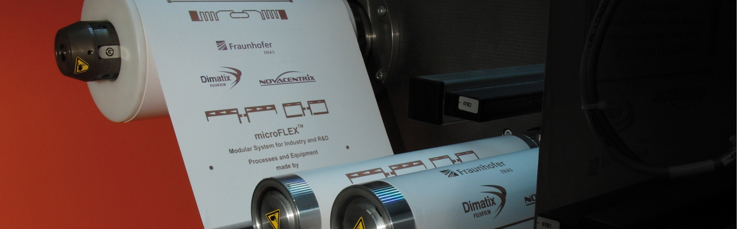
| Inkjet | sheet-fed, web-fed | |
| Aerosol jet | sheet-fed | |
| Gravure | web-fed | |
| Screen | sheet-fed, web-fed | |
| Functionality formation by sintering | thermal, IR, UV, laser, IPL, electrical, chemical, plasma | |
| Materials | ||
| Inks | conductive inks: Ag, Cu, Au, C, Zn, ..., semiconductive inks (organic and oxide-based), dielectric inks (organic) | |
| Substrates | polymer films (PET, PEN, PI, PC, PVC, PP, ...), paper (uncoated and coated), congurated cardboard, glass, ceramics, textiles, sheet metal, rubber | |
For your support, we operate the »Chemnitz Inkjet Technikum« offering the following research and development services: