28. Chemnitzer Seminar

We invite you to our

CHEMNITZER SEMINAR
»Materials and Technologies for MEMS Packaging«

on June 12 and 13, 2018
Venue: Fraunhofer ENAS, Technologie-Campus 3, 09126 Chemnitz


Smart systems are becoming more and more important in our daily life, e.g. in cars, security applications, medical engineering, condition monitoring, logistics and other applications. A major bottleneck, however, is the packaging of the sensitive microstructures on different levels to allow them to withstand even harsh environments and meet the competitive market requirements. In 2018 advanced electronic packaging materials, novel processes and technologies will be highlighted within the 28th Chemnitzer Seminar. On June 14, our cooperation partner Electronic Design Chemnitz GmbH will held a workshop about »Smart Sensor Technologies«. Find more information online: www.ed-chemnitz.de.

Program

Tuesday, June 12, 2018

12:30 – 12:40 pm

Welcome

Dr. Maik Wiemer, Fraunhofer ENAS

12:40 – 1:10 pm

Keynote: Materials for LED packaging

Dr. Norwin von Malm, OSRAM Opto Semiconductors GmbH

1:10 – 1:40 pm

New soldering pastes for diffusion based joining technologies

Steffen Käss, Heraeus Deutschland GmbH & Co. KG

1:40 – 2:10 pm

Materials for wafer level packaging, MEMS & semiconductor assembly

Ruud de Wit, Henkel Electronic Materials NV

2:10 – 2:40 pm Poster presentation, coffee break and networking

2:40 – 3:10 pm

Keynote: Glass frit wafer bonding for encapsulating monolithic integrated CMOS-MEMS devices

Roy Knechtel, X-FAB MEMS Foundry GmbH

3:10 – 3:40 pm

Glasfritbonding for pressure sensor

Dr. Timo Kober, Endress+Hauser SE+Co. KG

3:40 – 4:10 pm

Physical vapor deposition methods for Al/Pd based reactive multilayer systems

Ina Schmidt, Siegert Thinfilm Technology GmbH

4:10 – 4:40 pm

Smoothing of metallic thin films using advanced electropolishing technologies

Jean-François Vanhumbeeck, CRM Group

4:40 – 5:10 pm

Electroforming and hot embossing of micro- and nanostructured inserts for the manufacturing of biomimetic surfaces

Dr. Markus Guttmann, KIT – Karlsruhe Institute of Technology

5:10 – 5:40 pm

Research Fab Microelectronics Germany FMD

Dr. Stephan Guttowski, Forschungsfabrik Mikroelektronik Deutschland


Program Wednesday, June 13, 2018

9:00 – 9:10 am

Welcome

Dr. Maik Wiemer, Fraunhofer ENAS

9:10 – 9:40 am

Keynote: Panasonic AIS R&D’s vision and strategy

Hidekazu Umeda, European Technology Center in Panasonic Industrial Devices

9:40 – 10:10 am

Ag-Sintering of bare dies for power devices as an alternative to AuSn soldering

Ralph Schachler, Finetech GmbH & Co. KG

10:10 – 10:40 am Poster presentation, coffee break and networking

10:40 – 11:10 am

Wafer bonding with novel method for improved post-bond alignment for high volume production in MEMS applications

Thomas Schmidt, SUSS MicroTec Lithography GmbH

11:10 – 11:40 am

Advances in High Vacuum encapsulation for MEMS packaging based on metallic bonding interfaces

Dr. Bernhard Rebhan, EV Group

11:40 – 12:10 am

Soldering of aluminum with rosin based and inorganic fluxes

Dr. Nils Kopp, Elsold GmbH

12:10 – 1:10 am Lunch

1:10 – 1:40 pm

Nanotechnology meets temperature-sensitive devices

Dr. Jan Freitag, CiS Forschungsinstitut für Mikrosensorik GmbH

1:40 – 2:10 pm

Discussion

from 2:10

Individual Lab and Window Tours

Registration

The registration is free of charge.

Please send an e-mail for registration with the information whether you would like to attend both days or only one (June 12th or 13th) to events@enas.fraunhofer.de until June 1, 2018.

Hotel

Until May 14, rooms in Hotel Chemnitzer Hof can be ordered by using the keyword: Seminar System Packaging. single room (incl. breakfast): 68 EUR Hotel Chemnitzer Hof, Theaterplatz 4, 09111 Chemnitz phone: +49 371 684-0 | info@chemnitzer-hof.de

How to reach us

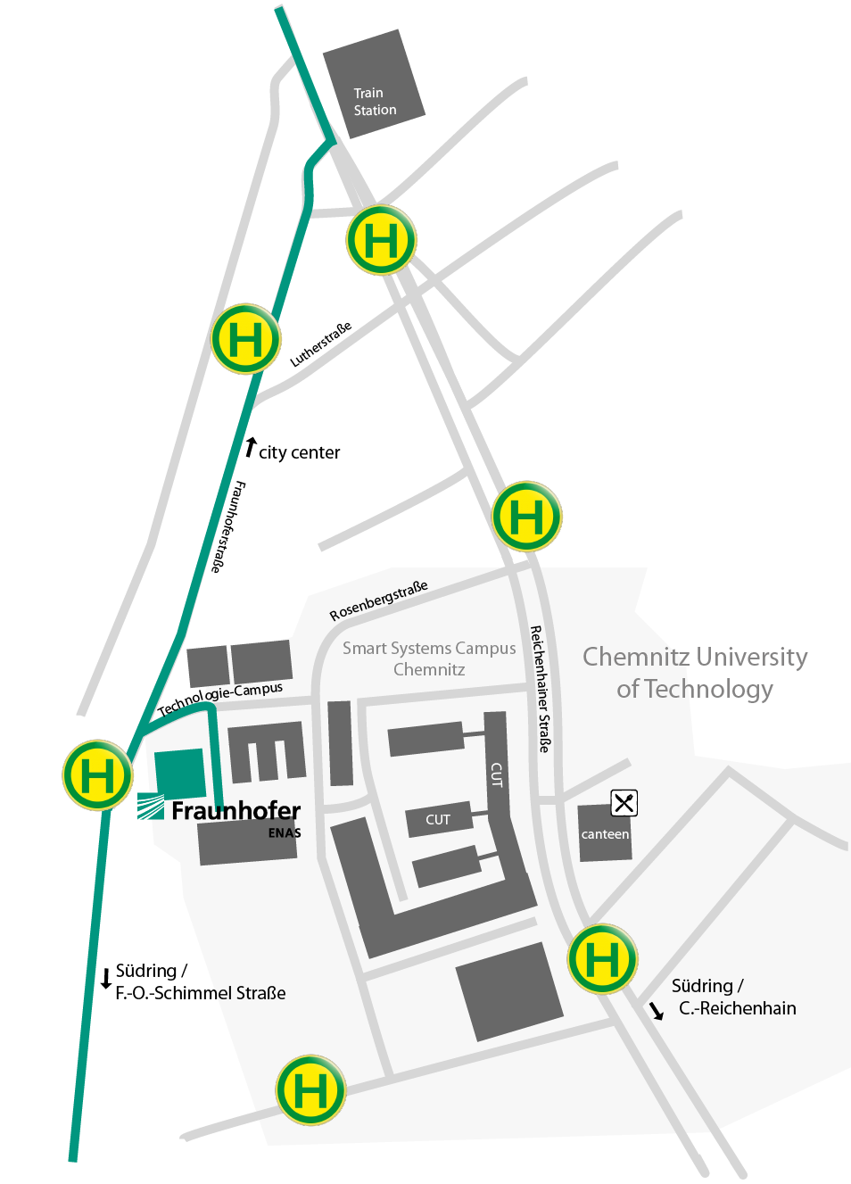
Fraunhofer ENAS, Technologie-Campus 3, 09126 Chemnitz

Attention - building site:
The access to Technologie-Campus is just possible via Fraunhoferstraße. From direction of A72, follow Neefestraße, turn right into Suedring and turn right into F.-O.-Schimmel-Straße. After the roundabout traffic you follow the Fraunhoferstraße.

Anfahrt 28. Chemnitzer Seminar
© Fraunhofer ENAS
ENAS_anfahrt_EN_detail

Fraunhofer Institute for Electronic Nano Systems ENAS

Technologie-Campus 3 | 09126 Chemnitz | Germany


phone: +49 371 45001-0

fax: +49 371 45001-101

info@enas.fraunhofer.de

www.enas.fraunhofer.de