 Fraunhofer Institute for Electronic Nano Systems
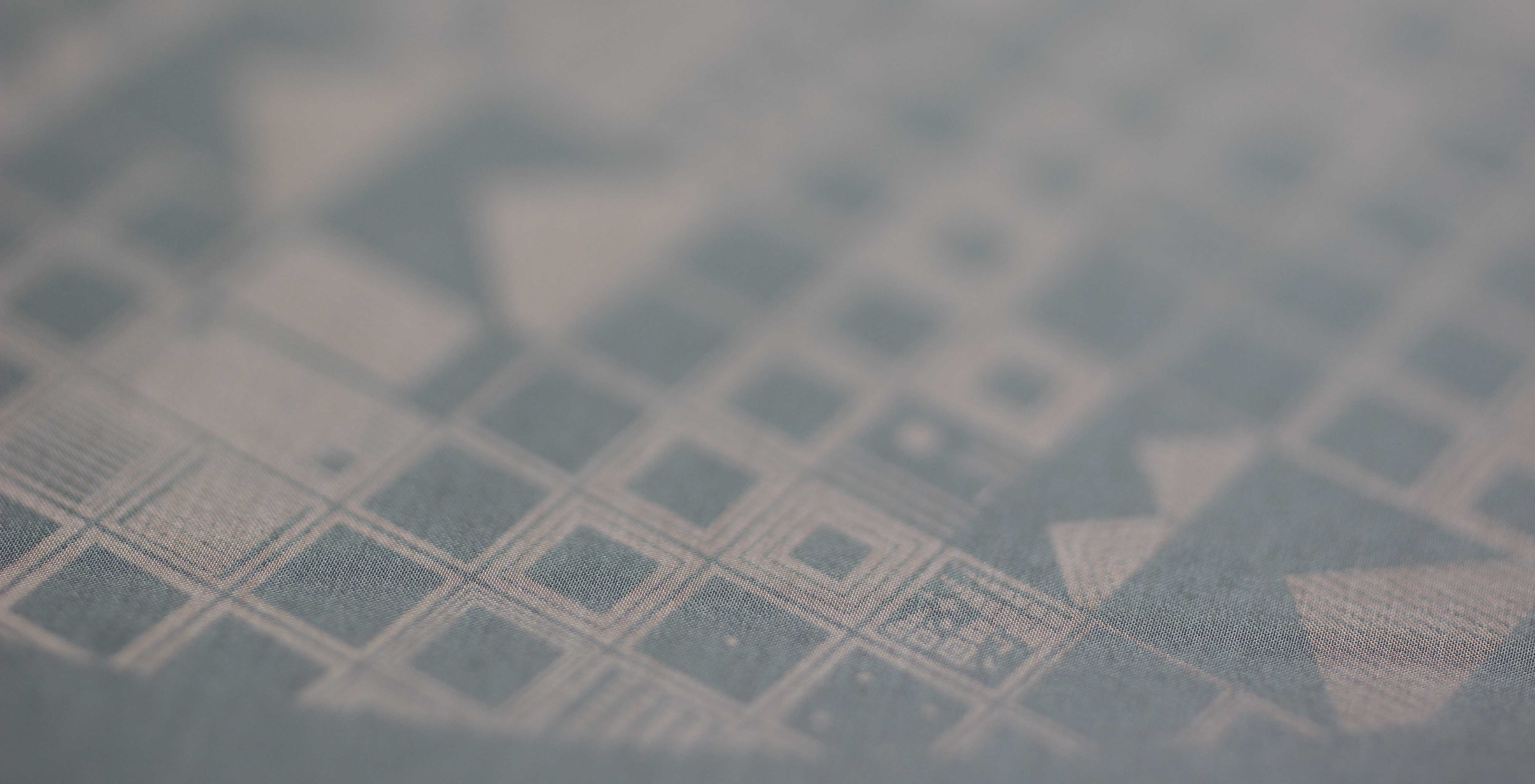
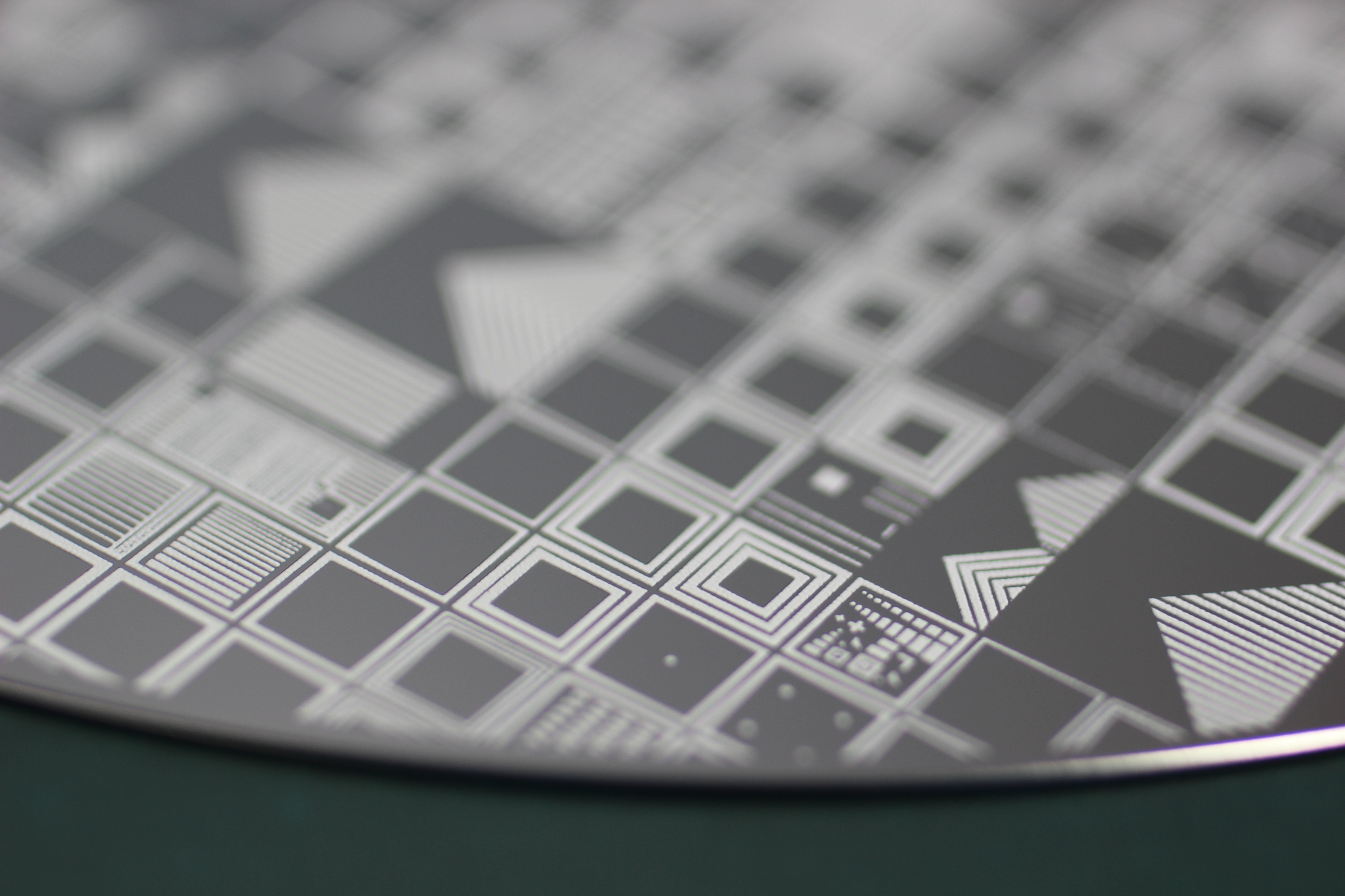
As a material transfer technology, screen printing is mainly used for selective deposition of intermediate layers for wafer bonding at Department System Packaging of Fraunhofer ENAS. With micro structured stencils, paste-like inks could be transferred to an electronic or semiconductor substrate through a polymeric or metallic screen. The specifications typically depend on the stencil openings, stencil thickness, and the screen size as well as on the pastes viscosity with involved ingredients like particle size, binder material and solvents.
Precise Equipment available
With a fully automatic and high precision in-line screen printer Reprint R29 Spectrum, glass frit pastes for wafer bonding but also other materials like solder pastes and adhesives could be clean room-like printed on substrates. The additional high performance screen printer DEK Horizon 03ix enhances the departments screen-printing capabilities by special features of precision wafer alignment, via filling, low volume dispensing module and trace stencil printing.
Broad field of research
Current research focuses on the minimal printable lateral- and vertical- feature sizes. Furthermore, the implementation of screen printable functional materials like conductive silver paste into microelectronic production processes is in focus of interest.
Substrates:
- Component frames ,silica wafers
- Glass wafers, ceramics, special substrates
- SMT Boards
- Flexible substrates Substrate
Application Examples:
- Hermetical wafer bonding
- Adhesive direct printing
- Electrical feed through
- MEMS Packaging
- Chip bonding / Flip-Chip bonding
- Assembly / Mounting
- Printed electronics
- Via in Pad
- Via filling SMT Boards
- Pin in paste
- Dispensing of adhesives or solder pastes