

Advances in electronics or sensorics by means of nanotechnology come usually along with the requirement on heterogenous fabrication technologies where nanodevices have to be modular and monolithically integrated on conventional systems such as MEMS, MOEMS or CMOS. As stated in the semiconductor roadmap materials like CNTs or graphene will be an essential ingredient to reach further miniaturization and higher performance as well as extended functionality in complex integrated circuits. For these heterogeneous technological scenarios, holistic approaches have to be applied ensuring suitable interfaces, compatible process conditions, packaging and at the end also scalable technologies.
At Fraunhofer ENAS we perform respective developments on integration technologies tailored for specific customer needs. We realize prototypes and perform technology transfer and know-how transfer to industrial partners. In the following some examples on projects are given:
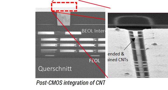
On-top of CMOS nanodevices: In the framework of prognostic health monitoring a holistic sensor concept is required to feed the digital lifetime models with current measurement data. In the smartSTAR cooperative BMBF project, a carbon nanotube-based sensor on top of an ASIC was integrated. Process design kits (PDK) were elaborated for a modular integration of CNT FET functionality. Specific for this feasibility study, the technology module was configured for strain sensing. Therefore, a novel surface technology for stress configurable nanomaterials was integrated. Accordingly, prestrained CNTs allowed to detect strains lower than 30 MPa. Compared to integrated silicon strain gauges we succeeded to show that sensitivity can be 3x higher, foot print of sensors can be reduced more than 10x and FET-based sensors can be added on-top-of CMOS in arbitrary BEOL level.
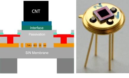
IR MOEMS with nanostructured nanomembranes: Next generation of micro-optical infrared (IR) sensors require advanced absorbers which fulfill tough technological and material requirements. A promising approach represent directly integrated vertically aligned carbon nanotubes (CNTs) as IR absorption and emitter layers. At MOEMS compatible processing conditions, we have shown high broadband absorption above 95% for λ = 2 … 12 μm on 5 µm thick CNT films. Due to the extremely low thermal mass of the functional layers in particular high speed IR applications are possible.
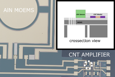
AlN MEMS with integrated CNT FET technology: another example for heterogeneous integration is a combination of piezoelectric MEMS devices with on-site signal processing based on CNT transistors. These concepts are in particular interesting for operation regimes with very small elongations where induced charge flows require on-site signal pre-processing. As a first step towards integrated systems, we have elaborated a process design kit for modular integration of CNT electronic components on AlN-based MEMS.
 Fraunhofer Institute for Electronic Nano Systems