Tokyo Big Sight West Hall 1/Conference Tower  /  December 09, 2020  -  January 25, 2021, online event until Jan 25, 2021 | onsite event Dec 9-11, 2020

MEMS Sensing & Network System 2021

Onsite-Online Hybrid Exhibition

MEMS Sensing and Network Systems 2021

Fraunhofer ENAS only attends in online exhibition

Permanent wafer bonding techniques

Permanent wafer bonding techniques are used in microelectronics and micromechanics to join thin, polished wafers made of different materials together - with or without additional intermediate layers.   

General requirements:

-        Low temperatures (< 400 °C)

-        Material compatibility

-        Mechanical stability

-        Most cases: hermetic sealing

-        Minimized bonding frame width

Piezoelectric actuators and sensors for medical technology

Microsystems based on piezoelectric aluminum nitride (AlN) offers the advantage of a high miniaturization potential. The technical developments include AlN-based microscanners with integrated position sensors for one or two-dimensional deflection of laser beams for application in high-precision, endoscopic systems for medical technology.

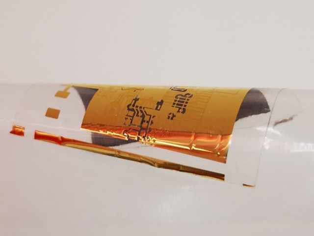
Ultra-thin and highly flexible PCB for tracking systems and wearables

An advanced, ultra-thin and highly flexible PCB of only 20 µm thickness.with multiple redistribution layers is presented. In the project Fraunhofer ENAS develops the flexible PCB of Parylene and MEMS with TSV.

The advantageous substrate properties are transparency, biocompatibility, and chemical stability to realize a versatile platform for flexible electronics.