 Fraunhofer Institute for Electronic Nano Systems
The focus of the applied research of department System Packaging are technologies both for the packaging of MEMS and NEMS in different packaging levels (wafer level, chip level, board level) and dimensions (2D, 3D) as well as for printing or micro- and nanostructuring of surfaces in microsystems technology. In addition to the standard wafer bonding methods such as silicon direct bonding, anodic, eutectic, adhesive and glass frit bonding also more novel wafer bonding methods such as laser assisted bonding, reactive bonding as well as low temperature and thermo-compression bonding are investigated and developed for specific fields of application. All wafer bonding techniques are characterized in terms of bonding quality, strength and hermiticity to ensure their suitability for certain applications.
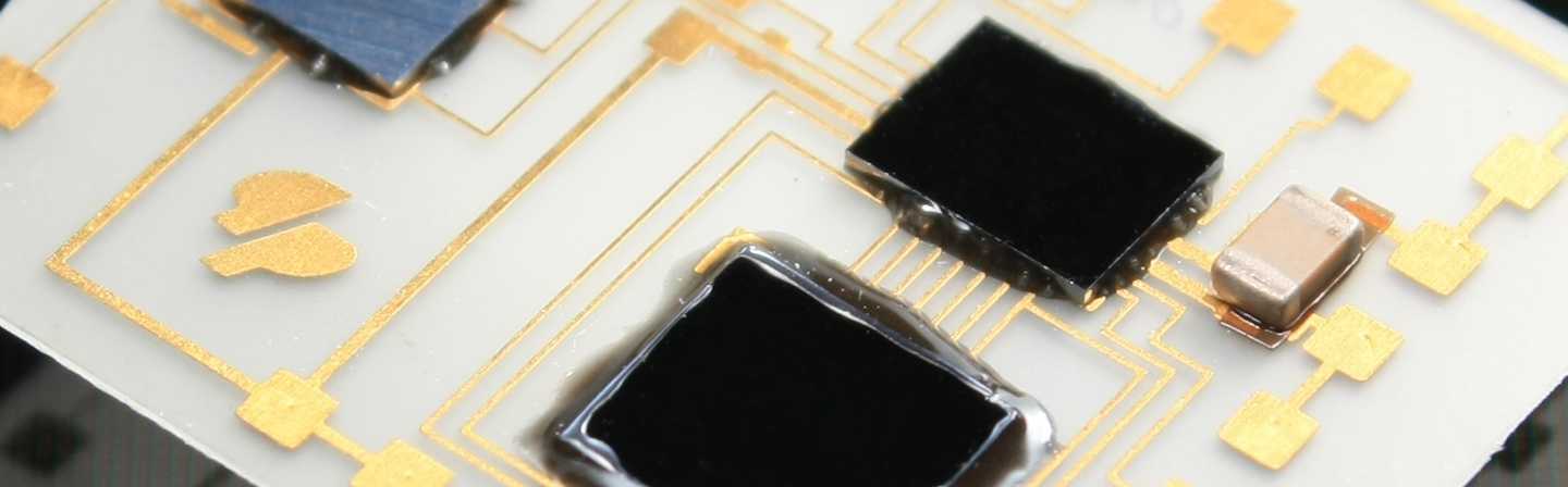
Component Integration
Hybrid integration on flexible substrates
© Fraunhofer ENAS
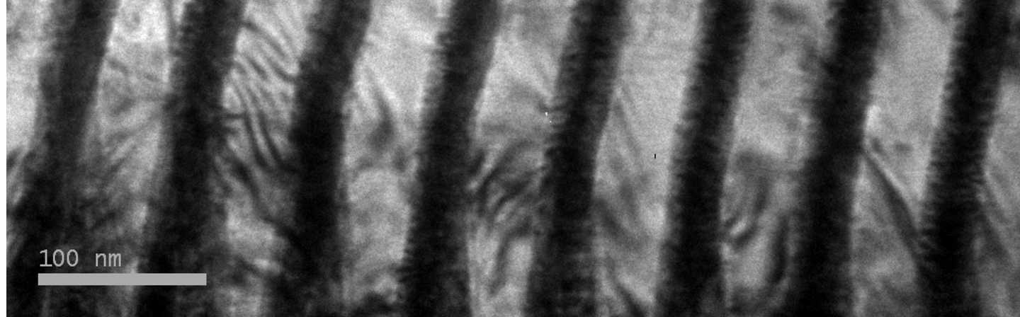
Innovative Waferbonding Processes
Nanoscale multilayer structure for wafer bonding
© Fraunhofer ENAS
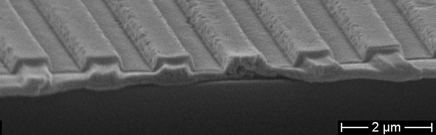
Surface Structuring
Nanostructures produced by Nanoimprint Lithography (UV-NIL)
© Fraunhofer ENAS
Department System Packaing - Research Fields
Assembly and connection technology for MEMS / NEMS