 Fraunhofer Institute for Electronic Nano Systems
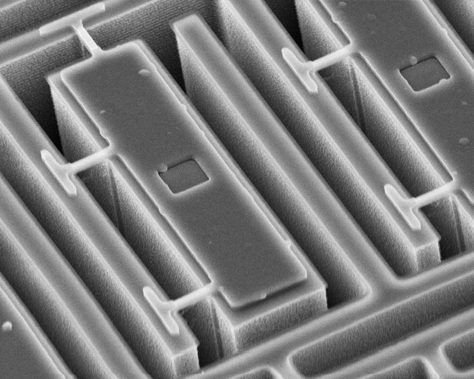
This technology platform uses standard Si wafers and enables the structuring of moving elements from the surface into the Si crystal. The electrical and mechanical contacting of the active structures takes place via a large number of thin metallic fingers on special carrier-layer systems. The electrical insulation is organized in the lateral and vertical direction by air gaps. Existing patents are related to post-process gap reduction and fixation methods in order to increase the capacitive sensitivity.
The multi-stage structuring process uses only plasma etching steps, is therefore fully CMOS-compatible and has already been demonstrated as a POST-CMOS MEMS process. In particular, the patented AIM* technology enables the fabrication of electrostatic actuators and capacitive sensors for the precise detection of very small movements in up to 3 dimensions.
The encapsulation can be carried out by means of thin-film encapsulation layer technology or wafer bonding. In addition to the standard version based on a glass-fried lid wafer with contact openings, technology variants with vertical vias were also investigated. The internal pressure can be adapted to the requirements of the applications in a white range.
Recent application examples are e.g. MEMS inertial sensors for precise measurement of inclination, acceleration and vibration as well as HF MEMS ohmic switches.
*Patent AIM: DE 10029012C2; U.S.No.10/296,771; PCT/DE01/02237
**Patent Gap reduction actuation: WO 2013/178343
***Patents Laser welding: DE 10 2015 008 119.5